CIMERA: Compute-in-Interconnect and Memory with Reconfigurable Precision for LLM Inference
July 15, 2026
Abstract
LLMs impose significant computational and memory demands, creating challenges for energy‑efficient inference across platforms ranging from data centers to power‑constrained edge devices. Weight precision plays a critical role in balancing inference accuracy, throughput, and energy consumption, while modern LLM workloads exhibit pronounced heterogeneity and tolerance that favors adaptive precision execution. This paper presents CIMERA, a reconfigurable‑precision LLM inference accelerator that integrates compute‑in‑interconnect and memory to mitigate the memory wall and enable precision‑aware execution. Compared to Nvidia H100, CIMERA delivers up to \(25\times\) and \(10\times\) higher energy efficiency for 1B and 13B models, respectively.
CIM, reconfigurable precision, LLM inference acceleration
1 Introduction↩︎
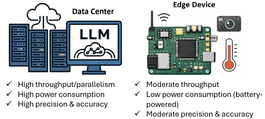
As LLMs are deployed across a wide spectrum of platforms from cloud-scale datacenters to power-constrained edge systems [1], there is a growing need for architectural techniques that can adapt model execution to diverse performance, accuracy, and energy requirements as shown in 1. Among the tunable hyperparameters, weight precision plays a critical role in determining the efficiency of LLM inference. While high-precision representations provide numerical robustness, they incur substantial storage and computation overhead. Conversely, low-precision representations (e.g., INT4) significantly reduce memory footprint and energy consumption.
Prior works [2]–[4] have shown that LLMs exhibit strong tolerance to reduced precision, particularly when precision is selectively applied based on layer sensitivity, tensor type, or inference phase. This observation has motivated the adoption of quantization and mixed-precision techniques as key enablers for efficient LLM deployment. Modern LLM inference workflows exhibit significant phase-level and layer-level heterogeneity, such as the differing numerical requirements between prefill and decode stages, or between attention and feed-forward network (FFN) layers [5].
Reconfigurable precision for model weights can be achieved through a combination of hardware and software co-design techniques. On the algorithmic side, multi-bit quantization schemes, grouped quantization, and progressive precision scaling allow weights to be encoded and accessed at variable bit-widths. On the hardware side, reconfigurable compute and memory structures enable dynamic selection of active bits during computation. Compared to fixed-precision accelerators, such designs offer finer-grained control over energy–accuracy trade-offs and can better exploit workload-dependent redundancy in LLM computations.
In this work, we propose CIMERA, an LLM inference accelerator architecture that integrates both in-memory and in-interconnect compute to mitigate the memory wall and support the deployment of LLM with weights of varying bit widths for aligning computational precision with workload requirements.
2 CIMERA Hardware Architecture↩︎
As 2 shows, the CIMERA hardware architecture adopts a chiplet-based design in which each chiplet contains PEs organized into a CT. Each CT integrates a 2D-mesh IPCN that interconnects multiple CIM PEs. The IPCN orchestrates data movement across PEs and performs DMAC, corresponding to the computation of attention scores (\(\mathbf{Q} \cdot \mathbf{K^T}\)). In contrast, the PEs execute SMAC, which implement the MVMs underlying the linear projections and feed-forward layers in the Transformer [6] architecture.

2.1 Processing Element (PE)↩︎
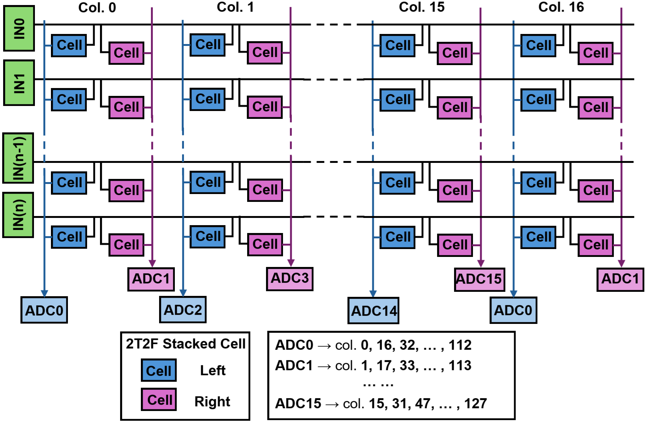
In this work, OS FeFET NVM array (Fig. 2) is fabricated, characterized, and incorporated as PE to perform SMAC. Each FeFET device stores a single neural network weight with up to 4‑bit precision (quad‑level cell, QLC), enabling compact multi‑bit weight representation within the memory array. Spatial bit-slicing [7] across adjacent columns is adopted for bit width \(>4\). FeFETs intrinsically exhibit non‑volatile behavior by exploiting the remanent polarization of the ferroelectric gate dielectric, which modulates the channel conductance. Due to the non‑volatility, model weights need to be programmed only once for a given LLM, thereby eliminating weight reconfiguration and reducing runtime overhead. Once initialized, the FeFET‑based PEs execute SMAC directly in the analog domain, leveraging the massive parallelism of crossbar structures and the high energy efficiency of CIM.
The FeFET offers strong compatibility with BEOL fabrication processes [8]. FeFET can be fabricated after completion of the FEOL CMOS logic transistors, enabling M3D integration, in which FeFET memory layers are vertically stacked above conventional CMOS logic through sequential fabrication. Consequently, all peripheral circuits, including control logic, ADC, and registers are implemented in the base FEOL CMOS tier without incurring additional silicon area overhead.
The SAR ADC [9] is adopted in the PE. It converts analog signals using an iterative binary search that sequentially determines each output bit via a capacitive DAC and a comparator. This architecture enables reconfiguration of the conversion resolution by truncating the SAR loop, allowing the converter to operate with fewer decision cycles and reduced switching activity at lower precision, thereby achieving lower energy consumption and shorter conversion time. The readout architecture employs 16 ADCs that are time-multiplexed across 128 memory columns using a strided sharing scheme (3). In other words, \(ADCi\) services columns \(i+16k\) for \(i \in \{0,\dots,15\}\) and \(k=0,\dots,7\). This organization enables uniform ADC utilization while reducing the overall ADC count.
2.2 Inter-PE Computational Network (IPCN)↩︎
The IPCN is designed to seamlessly integrate CIM PEs and to orchestrate efficient dataflow across the accelerator fabric for large‑scale LLM inference. In addition to serving as the on‑chip communication substrate, the IPCN embeds computation to support key LLM workload primitives. Operations such as DMAC, partial‑sum reduction, and activation functions are executed directly within the network routers, thereby reducing data movement and improving overall execution efficiency.
To support diverse LLM workloads and evolving execution patterns, the IPCN incorporates a reprogrammable ISA that provides fine‑grained control over data routing and in‑network computation. Each router instance features four planar ports for inter‑router communication, along with two pairs of AXI‑Stream interfaces that connect to the PEs. Global coordination across the 2D‑mesh IPCN is managed by the NMC, which programs the routers using a predefined instruction stream stored in the instruction memory.
In transformer-based LLM inference, the KV cache is used to store the key and value vectors generated by prior tokens, enabling reuse during the autoregressive decode phase and eliminating redundant recomputation of attention projections. In CIMERA, the SRAM scratchpad in each IPCN router is utilized to store the corresponding KV vectors for the layers mapped to the attached PE. By physically co-locating KV cache storage with in-network computation and data routing, the architecture enables low-latency, high-bandwidth access to KV vectors during attention score computation.
3 Mapping and Dataflow Orchestration↩︎
In practice, LLM workloads exhibit structured yet irregular computation and communication patterns across layers, tensors, and inference phases. Efficient execution on CIMERA requires a mapping strategy that explicitly aligns model structure, data locality, and execution order with the architectural organization of the PEs and the IPCN. By jointly optimizing spatial mapping and dataflow at the software level, the system can minimize data movement, localize reductions, and maximize parallelism, as demonstrated in [10], [11].
3.1 Mapping↩︎
The partitioned weight matrices \(\mathbf{W_Q}\),\(\mathbf{W_K}\),\(\mathbf{W_V}\), and \(\mathbf{W_O}\) are spatially distributed across the PE crossbar arrays, while the corresponding intermediate tensors \(\mathbf{Q}\), \(\mathbf{K}\), \(\mathbf{V}\), and \(\mathbf{O}\) are allocated to distributed on‑chip scratchpad memory. This separation allows weight matrices to remain stationary within the PEs, while intermediate data are accessed and reused efficiently during execution. To further improve data locality, intermediate activations are co‑located with their corresponding weight matrices. Specifically, each intermediate tensor is stored in the scratchpad memory associated with the IPCN routers attached to the PEs hosting its weight matrix. For example, the \(\mathbf{KV}\) matrix is placed in the scratchpads of the routers neighboring the PEs where \(\mathbf{W_K}\) and \(\mathbf{W_V}\) are mapped.
3.2 Dataflow↩︎
The intra-layer dataflow of LLM execution on CIMERA is structured around three fundamental communication patterns, each corresponding to distinct computational phases of the Transformer model: broadcast, reduction, and unicast. These patterns are orchestrated by the IPCN to efficiently match the data movement needs of attention computation and matrix–vector operations. During the projection stage, input embeddings are broadcast to the PEs hosting the weight matrices, enabling parallel evaluation of the \(\mathbf{QKV}\) projections across multiple PEs. Since each weight matrix is spatially partitioned and distributed across multiple crossbar columns, the resulting partial SMAC outputs are generated in parallel. Unicast communication is employed to compute the attention scores using DMAC within the IPCN.
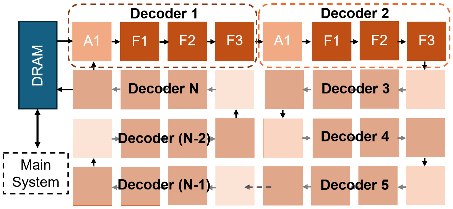
At the inter‑layer level, data propagation follows a serpentine execution topology as illustrated in 4, in which consecutive layers traverse across adjacent compute tiles. This topology aligns with the layer‑by‑layer execution characteristic of transformer inference and enables efficient pipelining of computation and data movement across the accelerator fabrics. The off‑chip DRAM serves as a centralized hub for external data exchange between the accelerator and the host system. With the static placement of model weights within the PEs, off‑chip memory accesses are confined to the prefill stage, where input tokens are ingested, and to the end of the decode stage, where the generated output is returned to the host.
| System Level | |||
|---|---|---|---|
| Bit-width | 64 | Frequency | 1 GHz |
| Compute Tile Level | |||
| IPCN Dimension | 32\(\times\)32 | PE # | 1024 |
| Macro Level (per unit Router-PE pair) | |||
| PE Array Dimension | 128\(\times\)128 | ADC # | 16 |
| Scratchpad Size | 32 KB | FIFO Size (each) | 128 B |
| DMAC # | 16 | I/O Pairs # | 6 |
4 System Evaluation↩︎
The proposed system was evaluated using a comprehensive hardware–software co‑verification methodology, with parameters in Table 1. Digital hardware components were implemented and functionally verified using Verilog HDL. Logic synthesis was performed with Synopsys Design Compiler, followed by physical implementation using Cadence Innovus for place‑and‑route. The power and area of SRAM scratchpad macros were obtained using CACTI [12]. For the PE, OS FeFET memory cells and a prototype array were fabricated using BEOL‑compatible M3D integration [8]. Measurement results from the fabricated array were used to develop a compact model, which accurately captures the electrical characteristics and behavior of the array, and incorporated into the system‑level simulation framework. End‑to‑end LLM inference was evaluated using a cycle‑accurate, instruction‑level simulator that implements the IPCN instruction set along with the proposed mapping and dataflow schemes [10]. The simulator captures both computation and communication behavior across compute tiles, enabling detailed analysis of system‑level performance, energy efficiency, and scalability under representative LLM workloads, as summarized in ¿tbl:tab:eval?.
c|c|c|c|c|c & Bit & Context Length & Throughput & Average & Efficiency
& Precision & (Input/Output) & (tokens/s) & Power (W) & (tokens/J)
& & 1024/1024 & 1416.4 & & 800.23
& & 2048/2048 & 789.4 & & 445.99
& & 1024/1024 & 969.2 & & 273.01
& & 2048/2048 & 566.4 & & 159.55
& & 1024/1024 & 594.1 & & 74.73
& & 2048/2048 & 361.9 & & 45.52
& & 1024/1024 & 520.5 & & 98.02
& & 2048/2048 & 348.4 & & 65.61
& & 1024/1024 & 309.8 & & 28.29
& & 2048/2048 & 221.9 & & 20.26
& & 1024/1024 & 171.2 & & 7.44
& & 2048/2048 & 128.6 & & 5.59
& & 1024/1024 & 333.9 & & 41.89
& & 2048/2048 & 237.2 & & 29.76
& & 1024/1024 & 192.4 & & 11.45
& & 2048/2048 & 146.2 & & 8.70
& & 1024/1024 & 104.1 & & 3.10
& & 2048/2048 & 82.72 & & 2.46
4.1 Performance Benchmarking↩︎
4.1.1 Throughput↩︎
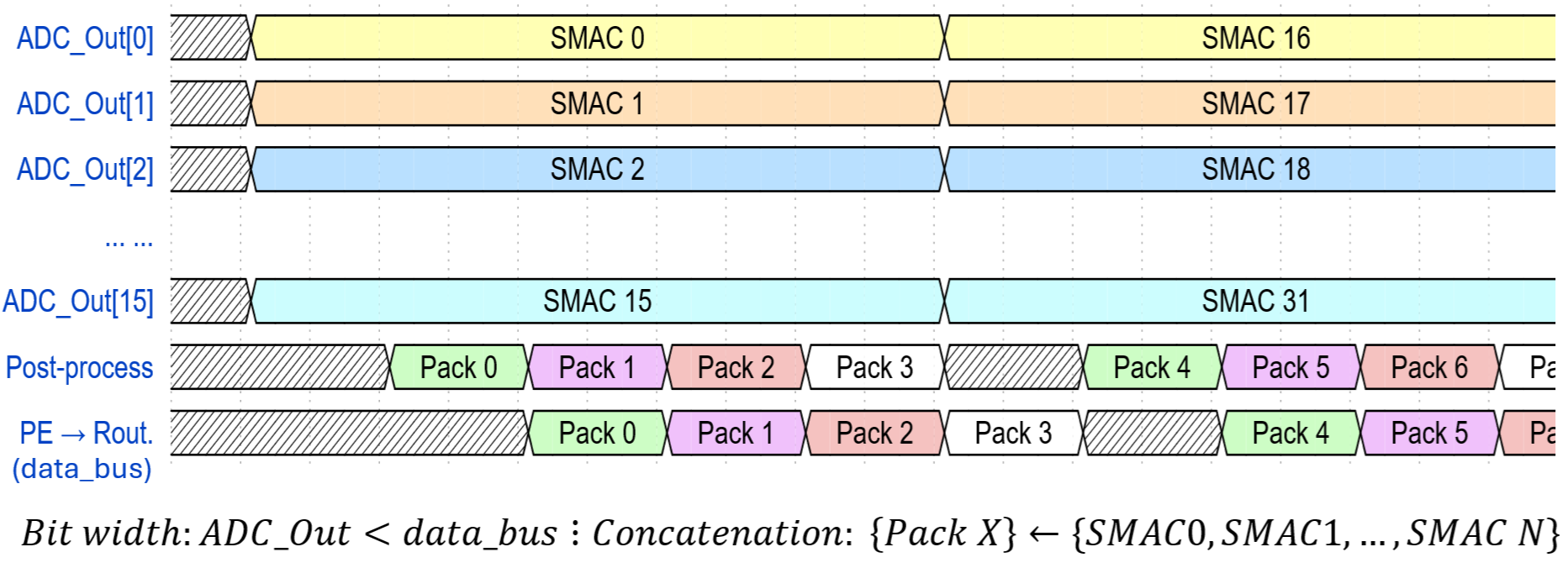
Across all evaluated models, lower weight precision consistently yields higher inference throughput. This throughput scaling is primarily attributed to the precision‑scalable SMAC execution in the PEs. At lower precision, fewer effective bit levels are activated during analog accumulation and peripheral conversion, thus reducing computation latency. Moreover, reduced vector widths decrease communication pressure within the IPCN, as more data can be concatenated and packed within each data packet (5).
As model size increases, the absolute throughput decreases due to a larger number of layers and increased inter‑layer traversal. However, the relative throughput gain from precision reduction remains consistent, demonstrating the scalability of CIMERA’s reconfigurable‑precision design. Increasing the context length from 1024 to 2048 results in a throughput reduction across all precision settings. This behavior is expected, as longer sequences increase attention computation and KV cache access overhead.
4.1.2 Power and Efficiency↩︎
System power consumption increases with higher weight precision across all models and context lengths. Since model weights are stored statically in non‑volatile PEs, power scaling is dominated by computation and communication precision rather than repeated off-chip memory accesses. Compared to fixed‑precision designs, CIMERA allows sacrificing numerical fidelity for energy efficiency. Moreover, with chiplet design and LLM workloads intrinsically executed in a sequential layer-by-layer manner, the power gating of idle chiplets enables sub-linear power scaling with respect to LLM size. Comparing to Nvidia H100, CIMERA achieves better average energy efficiency across different LLM sizes, from 1B (273 vs 11.2 tokens/J) to 13B (11.5 vs 1.2 tokens/J) at similar throughput.
4.2 Macro Power and Area↩︎
2 summarizes the power and area breakdown of the hardware macros. The CIM array in a PE occupies the largest fraction of area as the OS FeFET crossbar arrays integrate high‑density non‑volatile weight storage along with analog computation capability. Although the ADCs are a major contributor to power, their area is not included in the planar footprint since they are implemented in the underlying FEOL CMOS tier and the FeFET memory layers are vertically integrated above the ADCs using M3D integration. Thus, peripheral circuit complexity is effectively decoupled from array scaling.
| Macro\(^\#\) | Power (\(u\)W) | Breakdown | Area (mm\(^2\)) | Breakdown |
|---|---|---|---|---|
| CIM Array | 120 | 3.45% | 0.14 | 76.9% |
| ADCs* | 3200 | 92.20% | 0.074* | N/A |
| Scratchpad Mem. | 47 | 1.35% | 0.013 | 7.2% |
| Router | 105 | 3.00% | 0.029 | 15.9% |
| Total | 3457 | 100% | 0.182 | 100% |
| (Router-PE pair) |
\(^\#\)Technology node: 7 nm; Area per CT: 186.4 mm\(^2\)
Total of 16 units, not contributing to area due to M3D
5 Conclusion↩︎
By exploiting the inherent tolerance of LLMs to reduced and heterogeneous numerical precision, CIMERA enables flexible trade‑offs among accuracy, throughput, and energy efficiency. Through comprehensive hardware–software co‑verification and system‑level benchmarking, scalable improvements in both throughput and energy efficiency are demonstrated as weight precision is reduced, across models with varying context lengths and parameter counts. Compared to fixed‑precision accelerators, CIMERA provides a flexible architectural substrate that aligns computational precision with workload heterogeneity, enabling efficient deployment from edge devices to data‑center‑class systems. It achieves better average energy efficiency across LLM 1B (273 vs 11.2 tokens/J) to 13B (11.5 vs 1.2 tokens/J) at similar throughput as comparing to the Nvidia H100. This demonstrates the effectiveness of scaling up CIM with compute-in-interconnect.