ChipVerilog: A Large-Scale OpenCores-Derived Benchmark for LLM-Based Verilog RTL Generation
July 12, 2026
Abstract
Large language models have shown strong potential for Verilog RTL generation. However, many existing benchmarks are built from short, self-contained module-level tasks. These tasks are useful for controlled evaluation, but they do not fully capture the code scale, hierarchy, and module interactions found in practical IP and processor-core RTL. We present ChipVerilog, a description-to-Verilog generation benchmark built from OpenCores IP/core designs. The benchmark contains 64 generation targets from five design families: OR1200, double-precision FPU, MIPS-16, I2C, and CORDIC. It includes both single-module targets and cross-module targets that instantiate or interact with other RTL modules. Several targets exceed 1,000 lines of Verilog, making ChipVerilog substantially larger and structurally more complex than typical module-level suites. Each benchmark instance is constructed from a pair of specification documents and reference RTL. We extract the target functionality, write a detailed natural-language description, and manually review the description for correctness and clarity. Generated RTL is checked by compilation and validated through equivalence checking for local modules, or by simulation for integrated IP/core targets. Results show that large-scale RTL remains challenging, especially for hierarchical and cross-module designs.
1 Introduction↩︎
Recent advances in large language models (LLMs) have significantly accelerated research in hardware design automation, with promising results in Verilog RTL generation [1], [2], code optimization [3]–[5], debugging [6], [7], and verification assistance [8]–[10]. These developments suggest that LLMs have the potential to become useful assistants in digital design workflows, where engineers traditionally translate specifications into RTL, refine implementations, and validate correctness under complex architectural and verification constraints. Crucially, the development and refinement of these models depend heavily on specialized hardware benchmarks, which serve as the foundational training data and fine-tuning corpora for teaching LLMs how to generate hardware designs.
However, current LLM-based Verilog benchmarks remain largely centered on simple, single-module tasks [1], [11]–[13]. Most existing benchmark instances consist of short, self-contained RTL blocks often under 100 lines of code. Consequently, while models optimized on these datasets excel at generating isolated and flat code blocks, they fail to master the complex, deeply nested structural hierarchies inherent in modern production-grade chip designs. Furthermore, these benchmarks are typically evaluated through finite testbench simulations. While scalable, simulation-based evaluation only exercises behaviors covered by specific test stimuli, inherently leaving critical corner cases unverified. This creates a substantial gap relative to large-scale chip designs, where hardware modules are tightly integrated into broader intellectual property (IP) cores, interact via shared control paths, complex bus protocols, and memory hierarchies, and typically require formal verification guarantees.
To bridge this gap, we introduce ChipVerilog, a large-scale Verilog RTL dataset and benchmark designed for training and evaluating LLMs. ChipVerilog is constructed from manually curated OpenCores [14] IP and core designs, chosen for their stability, mature open-source RTL design status, and comprehensive specification documents. Each retained module is paired with a concise natural-language description derived from official documents and manually cleaned for consistency. Unlike existing datasets, ChipVerilog covers three levels of RTL targets: standalone modules, multi-module targets, and full-system targets. A standalone module is self-contained and does not instantiate other RTL modules. A multi-module target instantiates or interacts with external RTL modules, but its verification boundary is suitable for equivalence checking. A full-system target is an IP/core that integrates major subsystems such as processor pipelines, memory interfaces, bus logic, or protocol controllers. This multi-level benchmark forces LLMs to reason beyond simple code syntax, evaluating their capacity to preserve cross-module interfaces, coordinate functional dependencies, and complex integration logic.
The current version of ChipVerilog encompasses a diverse array of design domains, including arithmetic datapaths, control-intensive logic, protocol-driven interfaces, and subsystem-level integration. It contains 64 generation targets from five representative RTL design groups: a double-precision FPU, an OR1200 processor-core subsystem, a MIPS-16 processor core, an I2C controller, and a CORDIC computational core. In total, the benchmark includes approximately 20,400 lines of Verilog RTL, with a median file length of about 268 lines; 40 files exceed 200 lines, 7 exceed 500 lines, and 3 exceed 1000 lines. This scale and multi-layered structure distinguish ChipVerilog from existing simple RTL blocks, shifting the evaluation paradigm toward realistic design settings characterized by long code contexts, cross-module dependencies, and verification-driven constraints.
To summarize, our main contributions are as follows:
We identify the limitations of current LLM-based RTL benchmarks, including their focus on short standalone modules, limited IP/core-level context, and heavy reliance on finite testbench simulation.
We introduce ChipVerilog, a large-scale and hierarchy-aware Verilog RTL benchmark derived from manually curated open-source IP cores, covering standalone modules, multi-module targets, and full-system targets.
We propose a level-aware evaluation flow that uses equivalence checking for standalone modules and multi-module targets, and simulation-based validation for full-system targets.
We evaluate state-of-the-art LLMs on ChipVerilog and analyze their limitations in long-context, hierarchy-aware, and integration-aware RTL generation.
| Benchmark | Size | \(>\)1000 LOC | RTL Level | Module Interaction | Verification | Source |
|---|---|---|---|---|---|---|
| ChipGPT [15] | 8 | No | Module | None | Simulation | Hand-crafted |
| VeriGen_test [11] | 17 | No | Module | None | Simulation | Textbook / HDLBits |
| VerilogEval [1] | 156 | No | Module | None | Simulation | HDLBits |
| AutoChip [16] | 120 | No | Module | None | Simulation | HDLBits |
| ChipGPTV [17] | 30 | No | Module | None | Simulation | Hand-crafted |
| Evaluate_LLMs [18] | 8 | No | Module | None | Simulation | Textbook / Hand-crafted |
| RTLLM-v1 [19] | 30 | No | Module | None | Simulation | Academic / Hand-crafted |
| RTLLM-v2 [13] | 50 | No | Module | None | Simulation | Academic / Hand-crafted |
| ArchXBench [20] | 51 | No | Module / Partial IP | None | Simulation | Academic |
| CVDP [21] | 141\(^\dagger\) | No | Module / Partial IP | None | Test harness | Engineer-authored |
| RealBench [22] | 60 | No | IP | Cross-module | Simulation + Formal | Open-source IPs |
| ChipVerilog (ours) | 64 | Yes | IP/core | Cross-module | Equivalence + Simulation | OpenCores [14] |
3.2pt
\(^\dagger\) The reported CVDP size counts only its specification-to-RTL generation tasks; other task families in CVDP, such as debugging, verification, and Q&A, are excluded.
2 Related Work↩︎
A key challenge in LLM-based Verilog RTL generation is the lack of realistic benchmarks that reflect the scale, hierarchy, and integration constraints of practical hardware designs. Compared with software code, high-quality Verilog corpora are more limited in size, diversity, and contextual richness. Many existing datasets are built from short, self-contained modules with simplified specifications, making them convenient for controlled evaluation but less representative of real RTL development, where modules often interact through shared control paths, bus protocols, memory interfaces, and hierarchical design structures.
Existing description-to-Verilog benchmarks have made steady progress. Early works such as ChipGPT [15] and VeriGen [11] introduced natural-language-to-Verilog generation tasks based on small module-level designs, often from textbooks or hand-crafted examples. VerilogEval [1] and AutoChip [16] further standardized the evaluation of executables using HDLBits-style problems and testbench-based validation. Later benchmarks expanded the task scope: ChipGPTV [17] considers multimodal specifications, Evaluate_LLMs [18] provides a compact textbook and hand-crafted suite, and RTLLM-v1/v2 [13], [19] organize hand-crafted RTL tasks across multiple functional categories. More recent efforts move toward higher design realism. ArchXBench [20] targets architecture-oriented RTL synthesis, CVDP [21] covers generation, debugging, verification, and Q&A with structured test harnesses, and RealBench [22] evaluates IP-level Verilog generation using open-source IPs with both simulation and formal validation.
As summarized in Table 1, existing benchmarks are still dominated by short, module-level tasks. Recent IP-level benchmarks improve design realism, but large RTL targets with explicit hierarchy and cross-module dependencies remain limited. ChipVerilog addresses this gap by using OpenCores-derived IP/core designs with longer targets, including modules over 1000 lines and designs that instantiate or depend on other RTL components.
3 ChipVerilog↩︎
We introduce ChipVerilog, an OpenCores-derived benchmark for evaluating LLM-based description-to-Verilog generation on large-scale IP/core RTL. This section presents ChipVerilog in four parts: an overview of the benchmark workflow, the selected RTL designs, the construction of design specifications, and the validation methodology.
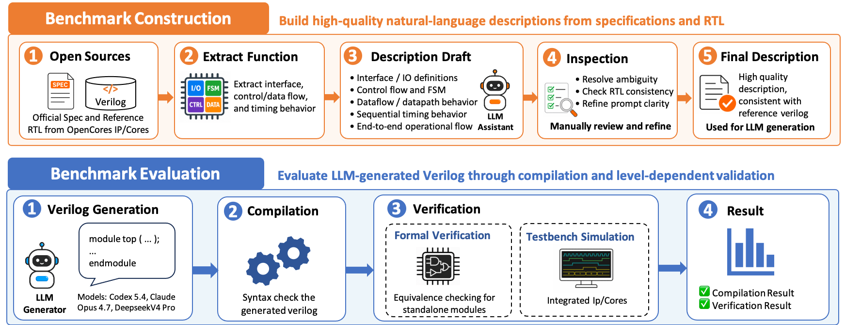
3.1 Overview↩︎
As illustrated in Figure 1, our methodology follows an end-to-end pipeline with two main phases: Benchmark Construction and Benchmark Evaluation. In the construction stage, we start from paired specification documents and reference Verilog RTL. We first extract the target module’s functionality, interfaces, and key behaviors from these sources, then organize the extracted information into a detailed natural-language description. The description is manually reviewed and revised to remove ambiguity and ensure consistency with the reference RTL. The approved description is then stored as the final benchmark prompt.
In the evaluation stage, the final description is given to an LLM to generate the target Verilog RTL. The generated code first undergoes syntax, compilation, and elaboration checks. Only compilable outputs proceed to functional validation. Depending on the target type, ChipVerilog uses equivalence checking for standalone modules and multi-module targets, and simulation-based validation for full-system targets.
3.2 Designs↩︎
The current release contains 64 generation targets distributed across five representative RTL design groups. Macro definition files, testbenches, and purely auxiliary files are excluded from the target set.
Floating-Point Unit (FPU): 9 targets covering double-precision arithmetic, IEEE-754 rounding, exception handling, and pipelined floating-point operations.
OR1200 Processor Core: 38 targets covering processor pipeline logic, cache and MMU components, exception handling, debug support, timer and interrupt logic, and Wishbone bus interfaces.
MIPS-16 Core: 11 targets covering a compact five-stage processor pipeline, including instruction fetch, decode, execution, memory access, write-back, register-file access, and hazard detection.
I2C Controller: 3 targets covering the top-level I2C master, byte-level control, and bit-level serial protocol control.
CORDIC Core: 3 targets covering iterative arithmetic logic, signed shifting, and CORDIC rotation-stage computation.
These design groups cover complementary RTL styles. The FPU and CORDIC subsets emphasize arithmetic datapath generation; the MIPS-16 subset captures compact pipeline organization; the I2C subset represents protocol-control logic; and the OR1200 subset provides the richest IP/core-level hierarchy, including integration-facing modules that instantiate or coordinate other RTL components. This composition allows ChipVerilog to evaluate description-to-Verilog generation across both standalone modules and modules embedded in larger processor or IP-level structures.
0pt
@c@c@ (lr)1-4Design& Lines& Hier.& Description fpu_add & 130 & single & Double-precision addition fpu_div & 412 & single &
Double-precision division fpu_double & 302 & multi(7) & Top-level double-precision FPU fpu_exceptions & 280 & single & IEEE-754 exception handling fpu_mul & 273 & single & Double-precision multiplication fpu_round &
91 & single & IEEE-754 rounding and packing fpu_sub & 221 & single & Double-precision subtraction fpu_addsub_pipeline & 367 & single & Pipelined add/subtract fpu_mul_pipeline & 270 & single & Pipelined
multiplication (lr)1-4Design& Lines& Hier.& Description EX_stage & 59 & multi(1) & Execution pipeline stage ID_stage & 290 & single &
Instruction decode stage IF_stage & 56 & multi(1) & Instruction fetch stage MEM_stage & 62 & multi(1) & Memory access stage WB_stage & 44 & single & Register write-back stage alu & 51 & single & 16-bit ALU
data_mem & 39 & single & Data memory hazard_detection_unit & 57 & single & Pipeline hazard detection instruction_mem & 80 & single & Instruction memory mips_16_core_top & 126 & multi(7) & Top-level MIPS-16
core register_file & 81 & single & Register file (lr)1-4Design& Lines& Hier.& Description i2c_master_top & 300 & multi(1) & I2C master top
module i2c_master_byte_ctrl & 344 & multi(1) & Byte-level I2C controller i2c_master_bit_ctrl & 576 & single & Bit-level I2C controller (lr)1-4Design& Lines&
Hier.& Description cordic & 379 & multi(4) & Configurable CORDIC core signed_shifter & 179 & single & Signed shift unit rotator & 253 & multi(2) & CORDIC rotation stage &
(lr)1-4Design& Lines& Hier.& Description or1200_alu & 468 & single & Execution-stage ALU or1200_cfgr & 234 & single & Configuration
register interface or1200_cpu & 806 & multi(13) & Main OR1200 pipeline core or1200_ctrl & 1052 & single & Instruction decode and control or1200_dc_fsm & 323 & single & Data-cache control FSM or1200_dc_ram & 189 &
multi(3) & Data-cache data array or1200_dc_tag & 181 & multi(3) & Data-cache tag array or1200_dc_top & 344 & multi(3) & Data-cache integration or1200_dmmu_tlb & 343 & multi(4) & Data-side TLB or1200_dmmu_top &
349 & multi(1) & Data MMU integration or1200_du & 1798 & multi(1) & Debug unit or1200_except & 579 & single & Exception/interrupt handling or1200_freeze & 203 & single & Pipeline freeze control or1200_genpc &
346 & single & Next-PC generation or1200_gmultp2_32x32 & 130 & single & 32\(\times\)32 signed multiplier or1200_ic_fsm & 265 & single & Instruction-cache control FSM or1200_ic_ram & 196
& multi(4) & Instruction-cache data array or1200_ic_tag & 198 & multi(4) & Instruction-cache tag array or1200_ic_top & 353 & multi(3) & Instruction-cache integration or1200_if & 189 & single & Instruction fetch
logic or1200_immu_tlb & 352 & multi(4) & Instruction-side TLB or1200_immu_top & 422 & multi(1) & Instruction MMU integration or1200_iwb_biu & 516 & single & Instruction-side Wishbone BIU or1200_lsu & 197 &
multi(2) & Load/store unit or1200_mem2reg & 433 & single & Memory-to-register logic or1200_mult_mac & 338 & multi(2) & Multiplier/MAC unit or1200_operandmuxes & 184 & single & Operand selection logic or1200_pic &
226 & single & Interrupt controller or1200_pm & 215 & single & Power-management unit or1200_qmem_top & 475 & multi(1) & QMEM local-memory interface or1200_reg2mem & 134 & single & Register-to-memory alignment
or1200_rf & 456 & multi(4) & Register file or1200_sb & 193 & multi(1) & Store buffer or1200_sprs & 477 & single & SPR interface or1200_top & 1065 & multi(13) & Top-level OR1200 wrapper or1200_tt & 223
& single & Tick timer or1200_wb_biu & 478 & single & Data-side Wishbone BIU or1200_wbmux & 168 & single & Write-back mux
Hier. denotes module hierarchy: single indicates a standalone target, while multi(n) indicates a target involving \(n\) instantiated or dependent submodules.
3.3 Specification Curation and Description Design↩︎
The quality and granularity of the input specification strongly affect the reliability of description-to-Verilog generation. Existing benchmarks often use concise functional requests, textbook-style summaries, or simplified HDLBits-style prompts. In contrast, ChipVerilog constructs benchmark-ready natural-language specifications by combining information from official specification documents and reference RTL implementations. Following Steps 2–5 in Figure 1, we curate each prompt through function extraction, description construction, and manual review.
Each specification is organized around interface, behavior, and execution information. The interface part defines input/output ports, signal widths, clock/reset assumptions, and macro-dependent interface variations. The behavior part describes the module’s dataflow, control flow, finite-state-machine transitions, arithmetic or protocol operations, configuration-dependent behavior, and sequential timing. The execution part summarizes the end-to-end processing flow, connecting the module inputs, internal control/data paths, state updates, and output behavior.
The manual review step checks whether the specification is consistent with the reference RTL and sufficiently clear for generation. During this process, we resolve ambiguous wording, remove irrelevant implementation noise, and avoid exposing the reference implementation verbatim. The resulting prompt captures the intended functionality and key implementation constraints of the target module while still requiring the model to synthesize the corresponding Verilog RTL.
Interface and boundary definitions: input/output ports, signal widths, clock/reset assumptions, macro-controlled ports, and integration-facing interface constraints.
Dataflow and datapath behavior: data dependencies, datapath transformations, arithmetic operations, mux selections, register updates, and output computation rules.
Control-flow and FSM behavior: control conditions, branch decisions, state transitions, enable/stall behavior, exception paths, and protocol-level actions.
Timing and sequential behavior: clocked update rules, pipeline stages, handshake timing, multi-cycle dependencies, and reset or hold behavior.
Operational flow: a step-by-step description that summarizes how the module processes inputs, updates internal state, coordinates control/data paths, and produces outputs.
3.4 Validation Flow↩︎
During evaluation, the finalized description is fed to an LLM to generate the target Verilog RTL. The generated code undergoes initial syntax validation, compilation, and elaboration. Designs that fail this stage are immediately classified as syntax failures and excluded from functional verification. For successfully compiled designs, ChipVerilog employs a level-aware validation strategy tailored to structural complexity, categorized into three distinct tiers.
For standalone modules, we apply formal equivalence checking against the reference RTL. This establishes a more rigorous correctness criterion than finite testbench simulation alone.
For multi-module targets, the generated module instantiates or interacts with external RTL modules, but its verification boundary remains local. We therefore replace only the target module with the generated RTL, while keeping the required submodules as reference implementations during equivalence checking. This setting validates whether the generated module preserves its interface behavior and functional interactions with surrounding RTL components.
For full-system targets, the target is an IP/core-level entry point that integrates major subsystems, such as processor pipelines, memory interfaces, or protocol controllers. Comprehensive formal equivalence checking becomes impractical for these targets because of the large state spaces. Therefore, full-system targets are evaluated through simulation-based validation using testbenches.
| Design | Claude | GPT-5.4 | DeepSeek | Design | Claude | GPT-5.4 | DeepSeek | ||||||
|---|---|---|---|---|---|---|---|---|---|---|---|---|---|
| 2-3 (lr)4-5 (lr)6-7 (lr)9-10 (lr)11-12 (lr)13-14 | Syn. | Func. | Syn. | Func. | Syn. | Func. | Syn. | Func. | Syn. | Func. | Syn. | Func. | |
| or1200_alu | or1200_reg2mem | ||||||||||||
| or1200_cfgr | or1200_rf | ||||||||||||
| or1200_cpu | or1200_sb | ||||||||||||
| or1200_ctrl | or1200_sprs | ||||||||||||
| or1200_dc_fsm | or1200_top | ||||||||||||
| or1200_dc_ram | or1200_tt | ||||||||||||
| or1200_dc_tag | fpu_mul | ||||||||||||
| or1200_dc_top | fpu_sub | ||||||||||||
| or1200_dmmu_tlb | fpu_add | ||||||||||||
| or1200_dmmu_top | fpu_div | ||||||||||||
| or1200_du | fpu_double | ||||||||||||
| or1200_except | fpu_exceptions | ||||||||||||
| or1200_freeze | fpu_round | ||||||||||||
| or1200_genpc | fpu_addsub_pipeline | ||||||||||||
| or1200_gmultp2_32x32 | fpu_mul_pipeline | ||||||||||||
| or1200_ic_fsm | EX_stage | ||||||||||||
| or1200_ic_ram | ID_stage | ||||||||||||
| or1200_ic_tag | IF_stage | ||||||||||||
| or1200_ic_top | MEM_stage | ||||||||||||
| or1200_if | WB_stage | ||||||||||||
| or1200_immu_tlb | alu | ||||||||||||
| or1200_wb_biu | data_mem | ||||||||||||
| or1200_wbmux | hazard_detection_unit | ||||||||||||
| or1200_immu_top | instruction_mem | ||||||||||||
| or1200_iwb_biu | register_file | ||||||||||||
| or1200_lsu | mips_16_core_top | ||||||||||||
| or1200_mem2reg | i2c_master_top | ||||||||||||
| or1200_mult_mac | i2c_master_byte_ctrl | ||||||||||||
| or1200_operandmuxes | i2c_master_bit_ctrl | ||||||||||||
| or1200_pic | rotator | ||||||||||||
| or1200_pm | signed_shifter | ||||||||||||
| or1200_qmem_top | cordic | ||||||||||||
3pt
4 Experimental Results↩︎
4.1 Experimental Setup↩︎
We evaluate ChipVerilog using generation targets collected from OpenCores [14] IP/core RTL designs. Each benchmark instance consists of a curated natural-language specification paired with a target Verilog module. Macro definition files, testbenches, and auxiliary support files are excluded from the generation target set. The benchmark includes standalone modules, multi-module targets, and full-system targets. We use Icarus Verilog [23] for syntax checking, compilation, elaboration, and simulation, and Yosys [24] for equivalence checking.
We evaluate three state-of-the-art LLMs: Claude Opus 4.5 [25], GPT-5.4 [26], and DeepSeek V4 Pro [27]. Generated RTL is first checked using Icarus Verilog (iverilog) for syntax validity, compilation, and elaboration. Outputs that fail this stage are counted as syntax failures and are excluded from
subsequent functional validation.
Following the validation strategy in Section 3.4, standalone modules and multi-module targets are evaluated using Yosys-based equivalence checking, where generated RTL replaces only the target module and required
submodules are kept from the reference design. Full-system targets are evaluated using iverilog-based testbench simulation. The full-system targets are or1200_top, mips_16_core_top, i2c_master_top,
fpu_double, and cordic; all remaining targets are evaluated by equivalence checking.
Following VerilogEval [1], we use the metric pass@k to evaluate functional correctness. pass@k represents the expected probability that at least one generated sample passes functional validation when randomly selecting \(k\) samples from \(n\) generated candidates:
\[\text{pass@k} := \mathbb{E}_{\text{Problems}} \left[ 1 - \frac{\binom{n-c}{k}}{\binom{n}{k}} \right]\]
where \(n\) denotes the total number of generated samples for a given problem, \(c\) denotes the number of functionally correct samples, and \(k\) is the number of selected candidates. We follow the standard unbiased estimator used in VerilogEval and set \(n=5\) in all experiments. Each of the five samples for a target is generated independently from the same benchmark prompt, without iterative feedback.
4.2 Overall Results↩︎
| Model | Syntax | Function | ||
|---|---|---|---|---|
| 2-3 (lr)4-5 | pass@1 | pass@5 | pass@1 | pass@5 |
| Claude Opus 4.5 [25] | 78.44% | 96.88% | 18.06% | 37.50% |
| GPT-5.4 [26] | 83.13% | 93.75% | 23.55% | 37.50% |
| DeepSeek V4 Pro [27] | 45.94% | 78.12% | 13.44% | 23.44% |

Tables 2 and 3 summarize the overall results. Across all models, syntax pass rates are much higher than functional pass rates, showing that current LLMs can often generate compilable Verilog but still fail to preserve the reference RTL behavior.
GPT-5.4 achieves the best pass@1 results, with 83.13% syntax pass@1 and 23.55% functional pass@1. Claude Opus 4.5 follows with 78.44% syntax pass@1 and 18.06% functional pass@1, while DeepSeek V4 Pro obtains 45.94% and 13.44%, respectively. Increasing the number of samples improves all models, especially on syntax: Claude reaches 96.88% syntax pass@5, GPT-5.4 reaches 93.75%, and DeepSeek reaches 78.12%. However, functional pass@5 remains much lower: 37.50% for both Claude and GPT-5.4, and 23.44% for DeepSeek. This gap shows that additional sampling helps recover syntax-level failures but still does not reliably produce behaviorally correct RTL.
This gap between syntax and functional correctness is central to our findings. Multiple samples can recover many syntax-level failures, but they do not reliably produce behaviorally correct RTL. For instance, Claude and GPT-5.4 both exceed 93% syntax pass@5, yet their functional pass@5 remains only 37.50%. The per-instance results further show that failures are more frequent on long and hierarchy-rich targets, including multi-module targets and full-system targets. These results indicate that ChipVerilog exposes challenges beyond compilability, requiring models to preserve control behavior, interface constraints, timing assumptions, and cross-module interactions.
4.3 Impact of Code Length↩︎
Figure 2 groups the results by reference RTL length. Syntax pass@1 remains relatively high across length groups, ranging from 61.6% to 80.7%, while functional pass@1 drops sharply as code length increases: 58.0% for targets below 100 lines, 17.7% for 100–300 lines, 3.2% for 300–500 lines, and 0.0% for targets above 500 lines.
These results indicate that increasing code length mainly challenges semantic correctness rather than syntactic generation. Current LLMs can still produce compilable Verilog for many long modules, but they often fail to preserve detailed control behavior, timing dependencies, interface constraints, and corner cases. Claude Opus 4.5 and GPT-5.4 maintain relatively strong syntax pass rates across most length groups, while DeepSeek V4 Pro is more sensitive to longer code. However, all three models exhibit near-zero functional correctness on long targets, highlighting the difficulty of long-context RTL generation.
4.4 Impact of Module Hierarchy↩︎
Table 4 reports hierarchy-level results aggregated across all evaluated models. Standalone targets and one-submodule targets achieve similar syntax pass@5 rates, 95.50% and 93.33%, respectively, with functional pass@5 rates of 44.14% and 46.67%. The main degradation appears for targets with two or more submodules. Although their syntax pass@5 remains 74.51%, both functional pass@1 and pass@5 are 0.00%. These results indicate that deeper hierarchy introduces challenges beyond compilability, including port wiring, width matching, timing alignment, and cross-module control/data coordination.
| Submodules | Tasks | Syntax | Function | ||
|---|---|---|---|---|---|
| 3-4 (lr)5-6 | pass@1 | pass@5 | pass@1 | pass@5 | |
| 0 | 37 | 77.48% | 95.50% | 23.06% | 44.14% |
| 1 | 10 | 61.33% | 93.33% | 25.33% | 46.67% |
| 2+ | 17 | 55.69% | 74.51% | 0.00% | 0.00% |
5 Conclusion↩︎
We presented ChipVerilog, an OpenCores-derived benchmark for evaluating LLM-based description-to-Verilog generation on large-scale IP/core RTL. Unlike short standalone-module benchmarks, ChipVerilog includes long RTL targets across standalone modules, multi-module targets, and full-system targets, covering floating-point units, processor cores, bus-control logic, and iterative arithmetic modules. Our results show a clear gap between syntactic validity and functional correctness. Although strong models achieve high syntax pass rates, their functional rates remain much lower, especially for long modules and targets involving multiple submodules. This indicates that current LLMs can often generate compilable Verilog, but still struggle with control behavior, interface consistency, and integration-level RTL semantics. ChipVerilog complements existing benchmarks by exposing these challenges in realistic OpenCores IP/core settings. Future work will expand the benchmark to more IP families and incorporate more detailed failure diagnosis and feedback-based repair evaluation.
6 Representative Prompt and RTL Example↩︎
This appendix provides one representative prompt example and one corresponding RTL excerpt from ChipVerilog. The example illustrates how a curated natural-language specification is paired with a non-trivial top-level Verilog RTL target. The complete benchmark artifact, including all prompts, reference RTL files, generated model outputs, validation scripts, and result summaries, is provided separately as supplementary material.
6.1 Prompt Example: fpu↩︎
6.1.0.1 Module Objective.
The module fpu is the top-level controller for a double-precision floating-point unit. It integrates the add, subtract, multiply, divide, rounding, and exception-handling blocks to produce IEEE-754 double-precision results.
The module accepts two 64-bit operands, an operation code, and a rounding mode. It detects a rising edge on enable, captures the operands and control fields into internal registers, routes the operation to the appropriate arithmetic
datapath, sends the selected intermediate result through rounding and exception handling, and finally publishes the result and status flags when the fixed-latency operation completes.
The supported operations are addition, subtraction, multiplication, and division. The supported rounding modes are round-to-nearest-even, round-toward-zero, round-toward-positive-infinity, and round-toward-negative-infinity.
6.1.0.2 Input Ports.
The module has the following input ports:
clk: clock signal that defines the sequential update timing of the top-level controller and all registered control paths.rst: reset signal that initializes internal registers, counters, result output, ready signal, and status flags to known values.enable: rising-edge start signal. A new operation is latched only whenenabletransitions from 0 to 1.rmode[1:0]: rounding-mode selector.2’b00: round to nearest.2’b01: round toward zero.2’b10: round toward positive infinity.2’b11: round toward negative infinity.
fpu_op[2:0]: floating-point operation selector.3’b000: addition.3’b001: subtraction.3’b010: multiplication.3’b011: division.Other encodings are unused.
opa[63:0]: first IEEE-754 double-precision input operand.opb[63:0]: second IEEE-754 double-precision input operand.
6.1.0.3 Output Ports.
The module has the following output ports:
out[63:0]: final IEEE-754 double-precision result. The value is selected from either the rounded normal datapath result or the exception-handling result.ready: asserted when the fixed-latency operation completes and the output result and status flags are valid.underflow: asserted when the exception-handling logic detects an underflow condition.overflow: asserted when the exception-handling logic detects an overflow condition.inexact: asserted when the result is inexact.exception: summary exception flag asserted when any exception-related condition is detected.invalid: asserted when an IEEE-754 invalid operation is detected.
6.1.0.4 Operation and Rounding Encoding.
The operation code fpu_op selects one of the arithmetic datapaths:
3’b000: addition.3’b001: subtraction.3’b010: multiplication.3’b011: division.
The rounding-mode input rmode selects the rounding behavior:
2’b00: round to nearest.2’b01: round toward zero.2’b10: round toward positive infinity.2’b11: round toward negative infinity.
6.1.0.5 Submodule Integration.
The top-level module instantiates six main submodules:
fpu_add: computes the addition datapath result.fpu_sub: computes the subtraction datapath result.fpu_mul: computes the multiplication datapath result.fpu_div: computes the division datapath result.fpu_round: rounds the selected intermediate sign, exponent, and mantissa according tormode.fpu_exceptions: checks special cases and exception conditions, and may override the rounded result.
The top-level control logic is responsible for selecting the active arithmetic result, forwarding the selected sign, exponent, and mantissa into the rounding module, and selecting between the rounded result and the exception result at completion.
6.1.0.6 Add/Subtract Routing.
For addition and subtraction, the top-level module uses the signs of opa and opb to decide whether the magnitude datapath should use the add block or the subtract block. For an addition operation, operands with the same sign
are routed to the addition datapath, while operands with different signs are routed to the subtraction datapath. For a subtraction operation, operands with different signs are routed to the addition datapath, while operands with the same sign are routed to
the subtraction datapath.
6.1.0.7 Fixed-Latency Completion.
The module uses operation-dependent latency counters to determine when the result is ready. The expected fixed latencies are:
addition: 20 cycles;
subtraction: 21 cycles;
multiplication: 24 cycles;
division: 71 cycles.
The ready output is asserted after the selected operation completes. At that time, out, underflow, overflow, inexact, exception, and invalid are valid.
6.1.0.8 Processing Flow.
The module operates as follows:
When
rstis asserted, clear the internal operand registers, operation registers, enable pipeline registers, counters, result output, ready signal, and status flags.Detect a rising edge on
enable.On the detected start pulse, latch
opa,opb,fpu_op, andrmodeinto internal registers.Decode the registered
fpu_opvalue to select addition, subtraction, multiplication, or division.For add/subtract operations, use the operand signs to select the appropriate magnitude datapath.
Enable the selected arithmetic datapath and generate intermediate sign, exponent, and mantissa values.
Select the active datapath output according to the registered operation code.
Send the selected sign, exponent, and mantissa to
fpu_round.Send the rounded result, post-round exponent, low-order mantissa bits, original operands, operation code, and rounding mode to
fpu_exceptions.When the operation latency expires, assert
ready.If the exception module requests an override, assign
outfrom the exception result; otherwise assignoutfrom the rounded result.Update
underflow,overflow,inexact,exception, andinvalidtogether with the final output.
6.1.0.9 Generation Requirement.
Generate synthesizable Verilog RTL for module fpu that matches the interface, submodule integration, operation routing, rounding path, exception path, fixed-latency ready behavior, and output flag behavior described above. Do not generate a
testbench or explanatory text.
6.2 RTL Excerpt: fpu↩︎
6.2.0.1 Purpose of This Excerpt.
The following RTL excerpt omits the complete module interface and internal signal declarations, since these are already described in the prompt. Instead, it focuses on representative implementation logic from the top-level fpu module,
including submodule integration, datapath result selection, operation-dependent latency control, enable-edge detection, ready generation, and final output/status update.
fpu_add u1(
    .clk(clk),.rst(rst),.enable(add_enable),.opa(opa_reg),.opb(opb_reg),
    .sign(add_sign),.sum_2(sum_out),.exponent_2(exp_add_out));

fpu_sub u2(
    .clk(clk),.rst(rst),.enable(sub_enable),.opa(opa_reg),.opb(opb_reg),
    .fpu_op(fpu_op_reg),.sign(sub_sign),.diff_2(diff_out),
    .exponent_2(exp_sub_out));

fpu_mul u3(
    .clk(clk),.rst(rst),.enable(mul_enable),.opa(opa_reg),.opb(opb_reg),
    .sign(mul_sign),.product_7(mul_out),.exponent_5(exp_mul_out));

fpu_div u4(
    .clk(clk),.rst(rst),.enable(div_enable),.opa(opa_reg),.opb(opb_reg),
    .sign(div_sign),.mantissa_7(div_out),.exponent_out(exp_div_out));

fpu_round u5(.clk(clk),.rst(rst),.enable(op_enable),    .round_mode(rmode_reg),
    .sign_term(sign_round),.mantissa_term(mantissa_round), .exponent_term(exponent_round),
    .round_out(out_round),.exponent_final(exponent_post_round));

fpu_exceptions u6(.clk(clk),.rst(rst),.enable(op_enable),.rmode(rmode_reg),
    .opa(opa_reg),.opb(opb_reg),
    .in_except(out_round), .exponent_in(exponent_post_round),
    .mantissa_in(mantissa_round[1:0]),.fpu_op(fpu_op_reg),.out(out_except),
    .ex_enable(except_enable),.underflow(underflow_0),.overflow(overflow_0),
    .inexact(inexact_0),.exception(exception_0),.invalid(invalid_0));


always @(posedge clk)
begin
    case (fpu_op_reg)
    3'b000:     mantissa_round <= addsub_out;
    3'b001:     mantissa_round <= addsub_out;
    3'b010:     mantissa_round <= mul_out;
    3'b011:     mantissa_round <= div_out;
    default:    mantissa_round <= 0;
    endcase
end

always @(posedge clk)
begin
    case (fpu_op_reg)
    3'b000:     exponent_round <= exp_addsub;
    3'b001:     exponent_round <= exp_addsub;
    3'b010:     exponent_round <= exp_mul_out;
    3'b011:     exponent_round <= exp_div_out;
    default:    exponent_round <= 0;
    endcase
end

always @(posedge clk)
begin
    case (fpu_op_reg)
    3'b000:     sign_round <= addsub_sign;
    3'b001:     sign_round <= addsub_sign;
    3'b010:     sign_round <= mul_sign;
    3'b011:     sign_round <= div_sign;
    default:    sign_round <= 0;
    endcase
end

always @(posedge clk)
begin
    case (fpu_op_reg)
    3'b000:     count_cycles <= 20;
    3'b001:     count_cycles <= 21;
    3'b010:     count_cycles <= 24;
    3'b011:     count_cycles <= 71;
    default:    count_cycles <= 0;
    endcase
end

always @(posedge clk)
begin
    if (rst) begin
        add_enable <= 0;
        sub_enable <= 0;
        mul_enable <= 0;
        div_enable <= 0;
        addsub_out <= 0;
        addsub_sign <= 0;
        exp_addsub <= 0;
        end
    else begin
        add_enable <= (add_enable_0 | add_enable_1) & op_enable;
        sub_enable <= (sub_enable_0 | sub_enable_1) & op_enable;
        mul_enable <= (fpu_op_reg == 3'b010) & op_enable;
        div_enable <= (fpu_op_reg == 3'b011) & op_enable & enable_reg_3;
            // div_enable needs to be high for two clock cycles
        addsub_out <= add_enable ? sum_out : diff_out;
        addsub_sign <= add_enable ? add_sign : sub_sign;
        exp_addsub <= add_enable ? { 1'b0, exp_add_out} : { 1'b0, exp_sub_out};
        end
end

always @ (posedge clk)
begin
    if (rst)
        count_ready <= 0;
    else if (enable_reg_1)
        count_ready <= 0;
    else if (count_busy)
        count_ready <= count_ready + 1;
end

always @(posedge clk)
begin
    if (rst) begin
        enable_reg <= 0;
        enable_reg_1 <= 0;
        enable_reg_2 <= 0;
        enable_reg_3 <= 0;
        end
    else begin
        enable_reg <= enable;
        enable_reg_1 <= enable & !enable_reg;
        enable_reg_2 <= enable_reg_1;
        enable_reg_3 <= enable_reg_1 | enable_reg_2;
        end
end

always @(posedge clk)
begin
    if (rst) begin
        opa_reg <= 0;
        opb_reg <= 0;
        fpu_op_reg <= 0;
        rmode_reg <= 0;
        op_enable <= 0;
        end
    else if (enable_reg_1) begin
        opa_reg <= opa;
        opb_reg <= opb;
        fpu_op_reg <= fpu_op;
        rmode_reg <= rmode;
        op_enable <= 1;
        end
end

always @(posedge clk)
begin
    if (rst) begin
        ready_0 <= 0;
        ready_1 <= 0;
        ready <= 0;
        end
    else if (enable_reg_1) begin
        ready_0 <= 0;
        ready_1 <= 0;
        ready <= 0;
        end
    else begin
        ready_0 <= !count_busy;
        ready_1 <= ready_0;
        ready <= ready_1;
        end
end

always @(posedge clk)
begin
    if (rst) begin
        underflow <= 0;
        overflow <= 0;
        inexact <= 0;
        exception <= 0;
        invalid <= 0;
        out <= 0;
        end
    else if (ready_1) begin
        underflow <= underflow_0;
        overflow <= overflow_0;
        inexact <= inexact_0;
        exception <= exception_0;
        invalid <= invalid_0;
        out <= except_enable ? out_except : out_round;
        end
end
endmodule
6.2.0.2 Discussion.
This excerpt highlights the integration-oriented nature of the fpu target. The model must generate not only arithmetic submodule instantiations, but also the control logic that captures inputs on an enable edge, routes add/subtract based on
operand signs, selects the active intermediate result, applies operation-dependent latency, invokes rounding and exception handling, and publishes the final result and status flags only when the operation is complete.