A 32-channel event-based bio-signal analog front-end with adaptive delta and pulse frequency encoding
July 14, 2026
Abstract
Low-power event-based AFEs are essential for building efficient, end-to-end neuromorphic signal processing systems. In this paper, we present an event-based AFE ASIC optimized for biomedical signal acquisition and encoding. The chip features 32 independently programmable input channels with dual-mode encoding mechanism outputs, comprising PFM and aADM circuits. The aADM encoder provides an auto-scaling mechanism that adapts the encoding data-rate based on the input signal envelope in real-time, enabling very high data compression for low-power information transmission. This approach paves the way toward adaptive wireless communication of neural signals for on-line processing in brain-computer interfaces. Fabricated in a 180 nm CMOS process, the proposed ASIC offers a highly configurable interface compatible with state-of-the-art SNN neuromorphic processors.
1 Introduction↩︎
SNNs implemented on bio-inspired neuromorphic hardware provide a low-power, event-driven signal processing paradigm, ideally suited for handling streaming data on the edge [1]–[3]. To leverage SNN-based data processing pipelines effectively, highly efficient event-based front-ends are required to convert analog sensory signals into the appropriate AER [4].
Several bio-signal processing systems have already been proposed in the past that included dedicated asynchronous circuits for low-power and low-latency event-based encoding [5]–[10]. However, typically those encoding circuits use fixed thresholds for data conversion. This strategy faces severe limitations when scaling the converters to large multi-channels or operating them long-term in real world BCI scenarios [11], [12]: fixing the thresholds too closely will generate large amounts of events for noisy signals; conversely, placing the thresholds too far apart to avoid encoding noise fluctuations will also reduce the encoding accuracy of the signal, degrading the downstream feature extraction. To overcome these limitations, we present the first realization of an aADM able to tune the encoding to the noise levels present in the bio-medical signal. Specifically, we designed and fabricated a 32-channel ASIC with configurable and adaptive sensory signal conditioning for efficient event encoding. The AFE circuits are explicitly optimized to operate at the low end of the frequency spectrum to process biomedical signals. The novel implementation of the aADM circuit dynamically adjusts the delta-modulation threshold in real-time, by following the envelope of the input signal. This allows it to encode only the meaningful parts of the signal, and to reject the noise floor present in the signal. By configuring the amount of adaptation, this circuit can adjust the data encoding and compression ratio at the sensor level, providing a trade-off between desired raw signal reconstruction accuracy and on-line information processing needs (e.g., to just detect the occurrence of a real action potential, or to classify specific spatio-temporal patterns). This approach makes this ASIC suitable for both scaling up to massive multi-channel bio-signal processing and encoding arrays, and for transmitting multi-channel asynchronous AER events with low-bandwidth and low-latency.
2 ASIC architecture↩︎
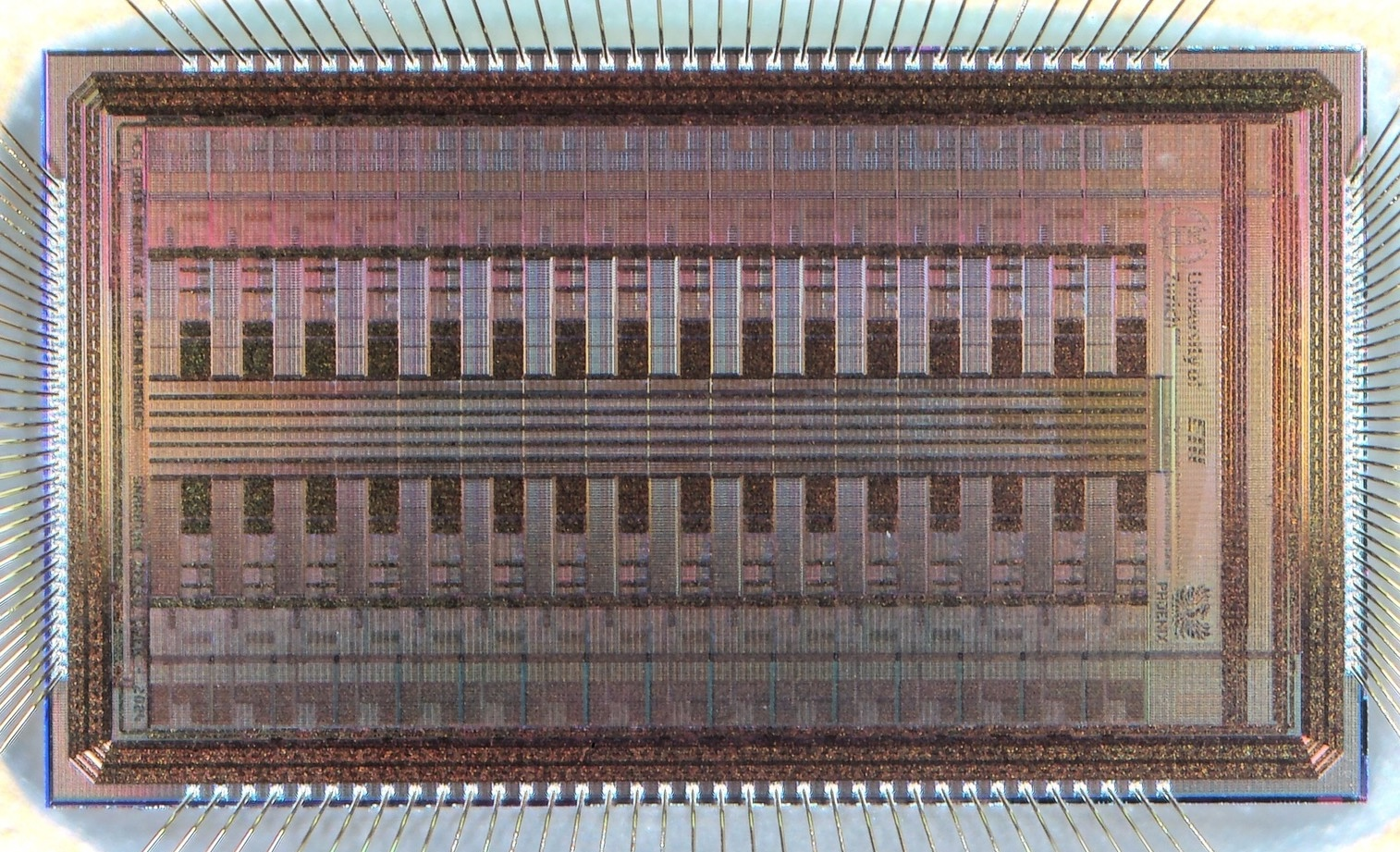
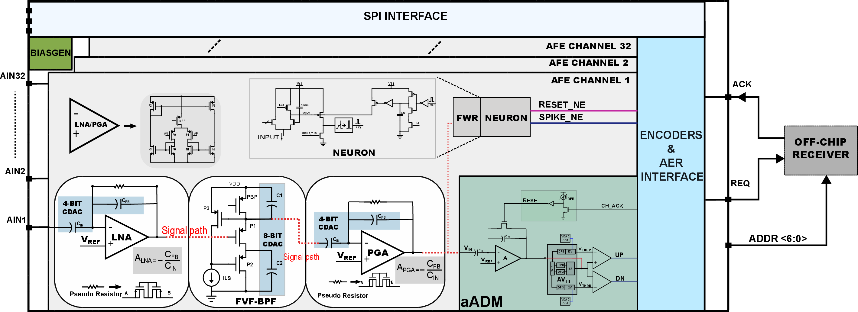
The chip comprises 32 analog processing channels that pre-condition the signal with amplification, filtering stages, and event-encoding circuits that convert the input signal into asynchronous discrete events, using parallel encoding methods: pulse-frequency modulation, via a low-power LIF neuron, and adaptive delta-modulation, via an aADM circuit. The analog circuit parameters can be programmed using an on-chip temperature compensated bias generator [13], [14]. All chip configurations, including the bias-generator, an 8 bit CDAC for filter parameters, and a 7 bit VDAC for aADM block controls, are programmed via a digital SPI based interface. The asynchronous output events generated by each channel are channeled through an arbiter tree and transmitted off-chip using the AER communication protocol [15], [16]. The ASIC measures \(3.22\,\text{mm} \times 5.67\,\text{mm}\) and is fabricated in the standard XFAB 180 nm. A micrograph of the fabricated chip is shown in Fig. 1.
An illustration of the ASIC building blocks and its signal processing pipeline is presented in Fig. 2. The processing chain for each input channel consists of four main stages: a LNA, a fourth-order BPF, a PGA, and the dual-mode event-based encoding block (aADM and PFM).
2.1 Pre-encoding circuit implementation↩︎
2.1.1 Low noise gain stages (LNA and PGA):↩︎
For modularity, both the LNA and PGA rely on the same OTA core, which is based on a wide input range current-mirror-type architecture to accommodate large input variations [17]. The amplifiers are operated in a closed loop as capacitive feedback amplifiers utilizing a DC-Servo loop implemented with pseudo-resistors [9], [18]. The LNA amplifies weak input signals with a tunable gain ranging from 0 dB to 22 dB, controlled by a 4 bit binary weighted CDAC.
2.1.2 The BPF↩︎
Every AFE channel has a 4th-order BPF with tunable center frequency \(\omega_{0}\) and \(Q\). The filter is based on a FVF topology (see Fig. 2) to achieve better noise performance due to the inherent current reuse present in the architecture [19]. The filter’s center frequency \(\omega_{0}\) is tunable with the on-chip bias generator [13]. The capacitors of this filter are implemented as an 8-bit CDAC. By configuring \(C_1\) and \(C_2\), \(Q\) and center frequency can be adjusted in a precise way with a resolution of \(C_{1,2}/256\) steps, as described in Eq. (1 ). \[\omega_0 = \sqrt \frac{ gm_1 \cdot gm_2}{C_1\cdot C_2}, \\ Q = \sqrt \frac{ gm_2 \cdot C_2}{gm_1\cdot C_1} \label{eq:omegaq}\tag{1}\]
As each filter’s center frequency and \(Q\) are programmable, they can be configured as a parallel filter bank or as identical parallel electrode interface channels. The PGA following the BPF adds additional gain to the signal but the combined frequency response now takes the response of the BPF.
2.2 aADM encoding↩︎
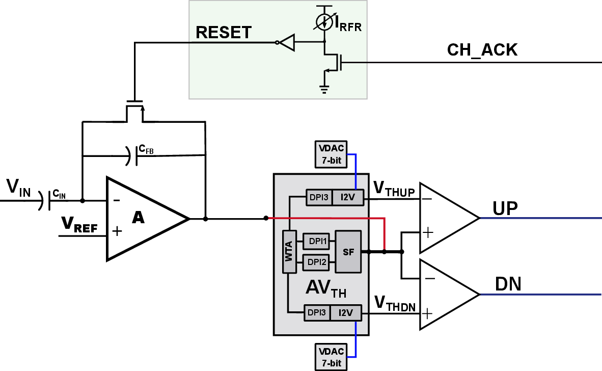
The basic ADM circuit [7] belongs to a class of level crossing ADCs where the sampling interval is adapted based on the characteristics of the coded signal [20]. In its classic form it comprises two comparators with a fixed threshold (termed as delta threshold) acting as a level shifter around a base line. This setup outputs an event based on the difference in the amplitude of a signal, when the change is compared with two known thresholds (termed as up- and down- delta thresholds) set by an on-chip VDAC to encode both upward and downward swings of the input. An ‘UP’ or ‘DN’ tag is attached to the output event based on the polarity of the change, i.e., if the signal has increased or decreased at the level crossing more than the set threshold. The on-chip AER interface produces a ‘REQ’ signal to transmit the address of the sending node off-chip (see Fig. 2). Once acknowledged off-chip, the chip-level acknowledge signal ‘ACK’ is converted back into a per-channel signal (‘CH_ACK’). This signal is gated with a current-controlled (\(I_{\mathrm{RFR}}\)) inversion stage to create a ‘RESET’ mechanism with a refractory period in each channel that resets the aADM circuit.
This approach asynchronously digitizes and encodes relevant changes in the input signal, based on the set delta threshold. The accuracy of conversion therefore depends on the chosen fixed delta-threshold. Low thresholds will produce a high data rate, allowing even lossless reconstruction, while higher thresholds will lead to lower data rates, at the cost of lower reconstruction accuracy. In real-world applications, such as long-term multi-channel monitoring in biomedical or BCI domains, input signals are naturally affected by noise, and the noise profile can change and drift with time. In these cases, a fixed delta threshold might become non-ideal. The solution implemented here is based on an adaptive scheme that changes the delta threshold based on the low frequency changes of the input signal envelope, but still encoding its high amplitude-high frequency fluctuations [21]. The schematic diagram of the circuit we designed and fabricated in the ASIC presented here is shown in Fig. 3.
2.2.1 Adaptive Delta threshold generation↩︎
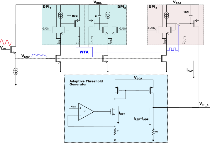
The adaptive delta threshold generation block consists of four stages. The input signal from the preceding signal conditioning stage (with gain and filtering circuits) flows into the adaptive delta generator circuit (Fig. 3, highlighted in grey) with a fixed gain of \(A=4\). Figure 4 presents the four stages of the delta generator. The first stage is an envelope extractor which is implemented using a subthreshold SF circuit (Fig. 4, left). This extracted envelope is then fed into two DPI circuits, which act as current-mode low-pass filters, when operated in the subthreshold regime [22], [23].
The output of the two DPIs are then compared with a current mode WTA circuit to detect a rapid change in signal and to adapt the threshold of the ADM. In the current silicon implementation, the capacitor used in DPI1 is \(99\) times that of DPI2 to produce a large difference in time constants between the two filters, so that the circuit can determine fast changing signals. The WTA picks the winner and triggers a sampling operation in DPI3 [21]. The output current of DPI3 therefore is proportional to the very low-frequency components of the input signal envelope, and neglects the fast transients (such as action potentials) present in the signal. This current is then added to or subtracted from the baseline threshold, encoded as current and generated by a current to voltage converter (marked as Adaptive Threshold Generator in Fig. 4). The composite current is then converted back to voltage within the same block, generating the final adaptive delta threshold voltage (VTHX). For the ‘UP’ threshold the adaptive current is added to the baseline, and for ‘DN’ one it is subtracted from the baseline.
2.3 Pulse frequency modulation↩︎
The PFM encoder is realized using an AdExp circuit [24] using previously proposed topology schemes [9]. This result is obtained by first converting the amplified and filtered voltage into a current, and then by sending it directly as input to the AdExp silicon neuron. The voltage-to-current conversion is carried out by a wide-range transconductance amplifier with source degeneration to extend the linearity. The current is then full-wave rectified and subsequently copied to the neuron input. As PFM encoding of signals has been amply described in the literature and demonstrated across many implementations, in this work we focus mainly on the aADM results. However, preliminary measurements on this chip proved this section to be functional as well.
3 Measurement results↩︎
The initial silicon measurements reported in this section verify the chip’s functionality.
3.1 Noise measurement↩︎
Noise analysis of a typical analog front end can be modeled as: \[v_{n,AFE}^{2} = v_{n,LNA}^{2} + \frac{v_{n,BPF}^{2}}{A_{LNA}^{2}} + \frac{v_{n,PGA}^{2}}{A_{LNA}^{2} A_{BPF}^{2}} + \frac{v_{n,ENCODER}^{2}}{A_{LNA}^{2} A_{BPF}^{2} A_{PGA}^{2}} \label{eq:noise}\tag{2}\] The overall input referred noise of the chain is dominated by the first stage in the chain, namely the LNA and its gain. The gain of the following stages helps in reducing the fractional term in Eq. 2 . As the primary objective of this chip was to demonstrate its on-chip adaptive compression capabilities, in the inherent trade-off of area, power and noise we allocated more area to the aADM circuit at the cost of higher noise levels in the LNA, which could, however, be further optimized if necessary (at the cost of more area).
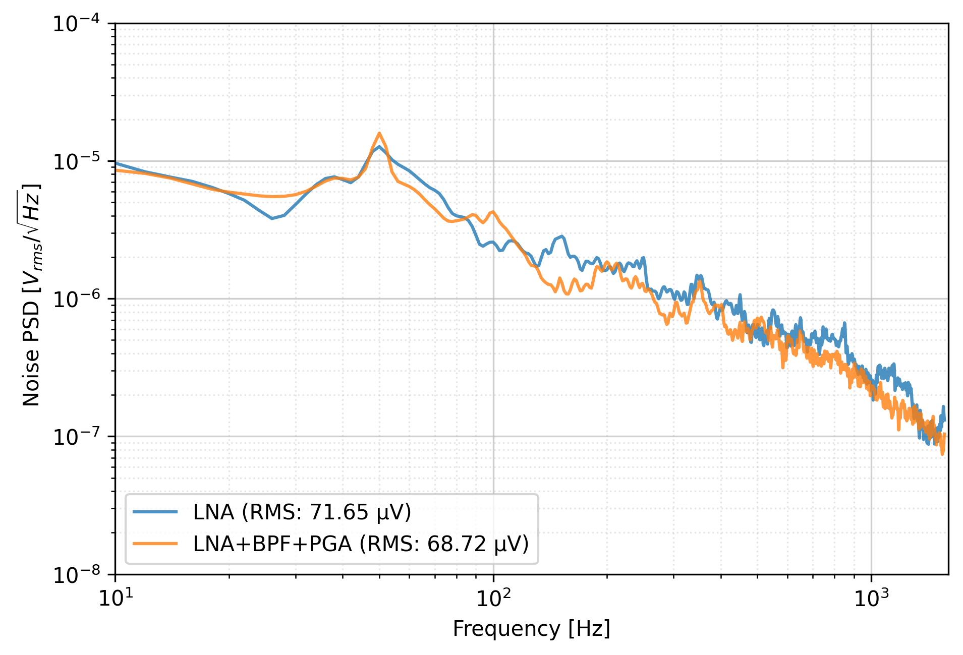
Figure 5: Input Referred Noise Power Spectral Density integrated from 10 Hz to 1.6 kHz..
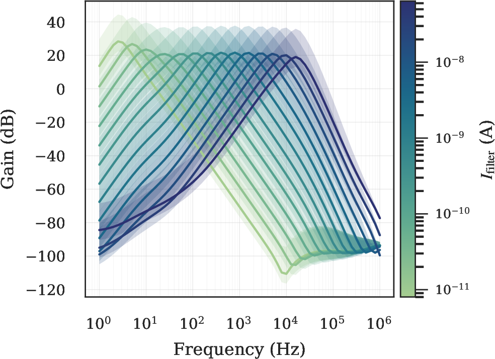
The initial silicon characterization of the AFE signal chain was performed to quantify the programmable gain control and noise performance. The measurement results of the gain and frequency response of the chain is shown in Fig. 6. The measurement of the LNA-BPF-PGA chain over a target biomedical bandwidth of 1.6 kHz demonstrated an input-referred noise power spectral density integrating to 68.72 \(\mu\text{V}_{\text{rms}}\).
3.2 Encoding↩︎

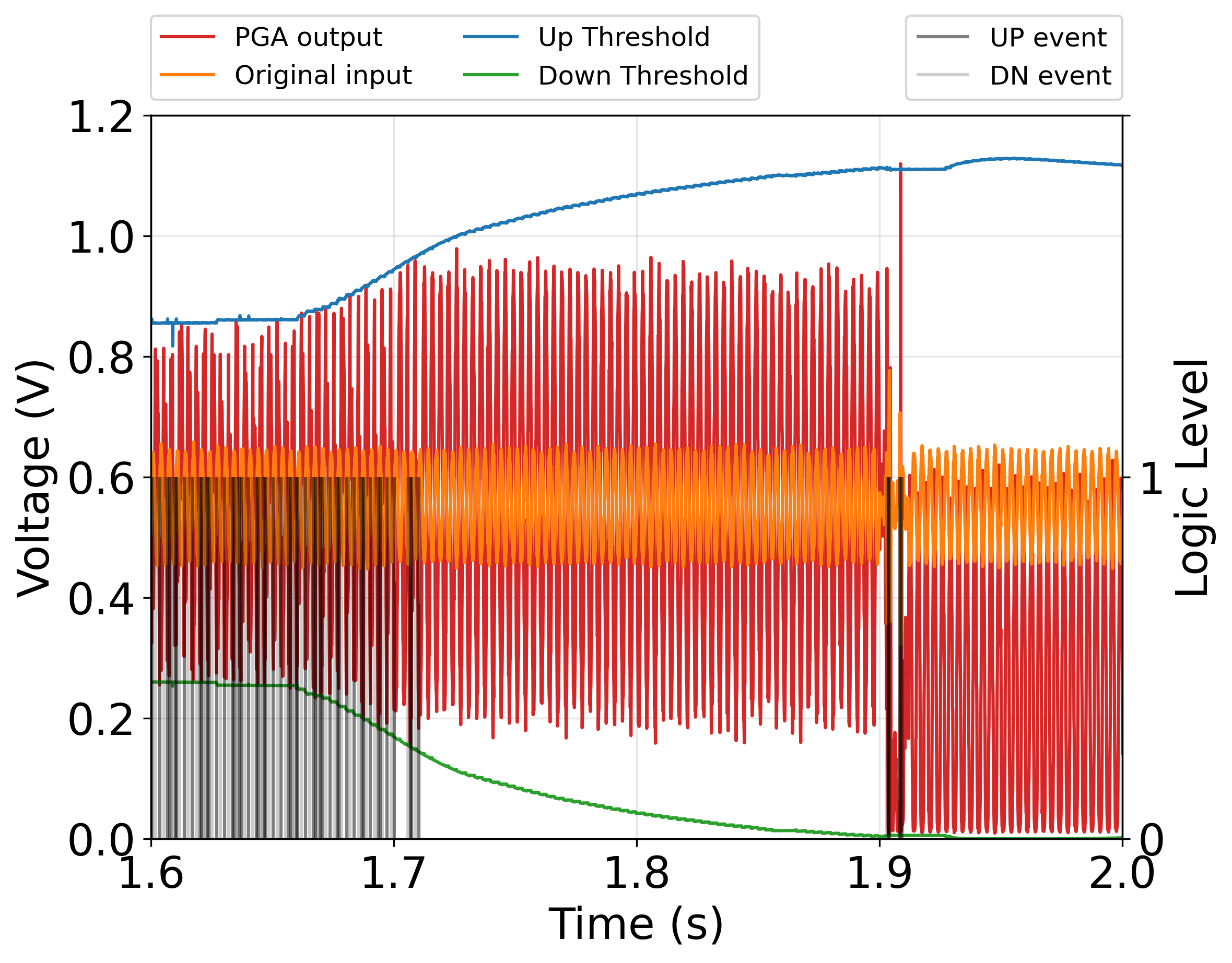
Figure 7: Circuit-level simulation of the aADM block showing changing threshold based on the input signal; () shows a noisy input signal with staircase amplitude, changing threshold, and corresponding encoded events. () Zoomed-in part of the simulation, with an additional pulse artificially added to the input signal, to represent an action potential or event of interest at t=1.9s. As expected, the encoder responds to this high-frequency input pulse even after the aADM has adapted to the highest noise levels..
A circuit-level simulation showing the internal signals of the adaptive delta threshold circuit is shown in Fig. 7 (a). Both an input signal (pure-tone sinusoid), amplitude modulated with a staircase function and added white noise, representing changing noise floors in a realistic control-input are shown. The input was first amplified though the gain stages before being fed into the adaptive generator block. The input to the adaptive generator block as well as the output delta (‘UP’ and ‘DN’) thresholds (depicted in blue and green lines) are depicted in relation to the input in Fig. 7 (a). The encoded events are presented as logic pulses showing the fast adaptation with changing noise floors in the staircase signal. Figure 7 (b) demonstrates that after adaptation, the addition of an event of interest (e.g., an action potential in a neural recording) will encode it reliably with additional events, despite having adapted to the high noise floor.
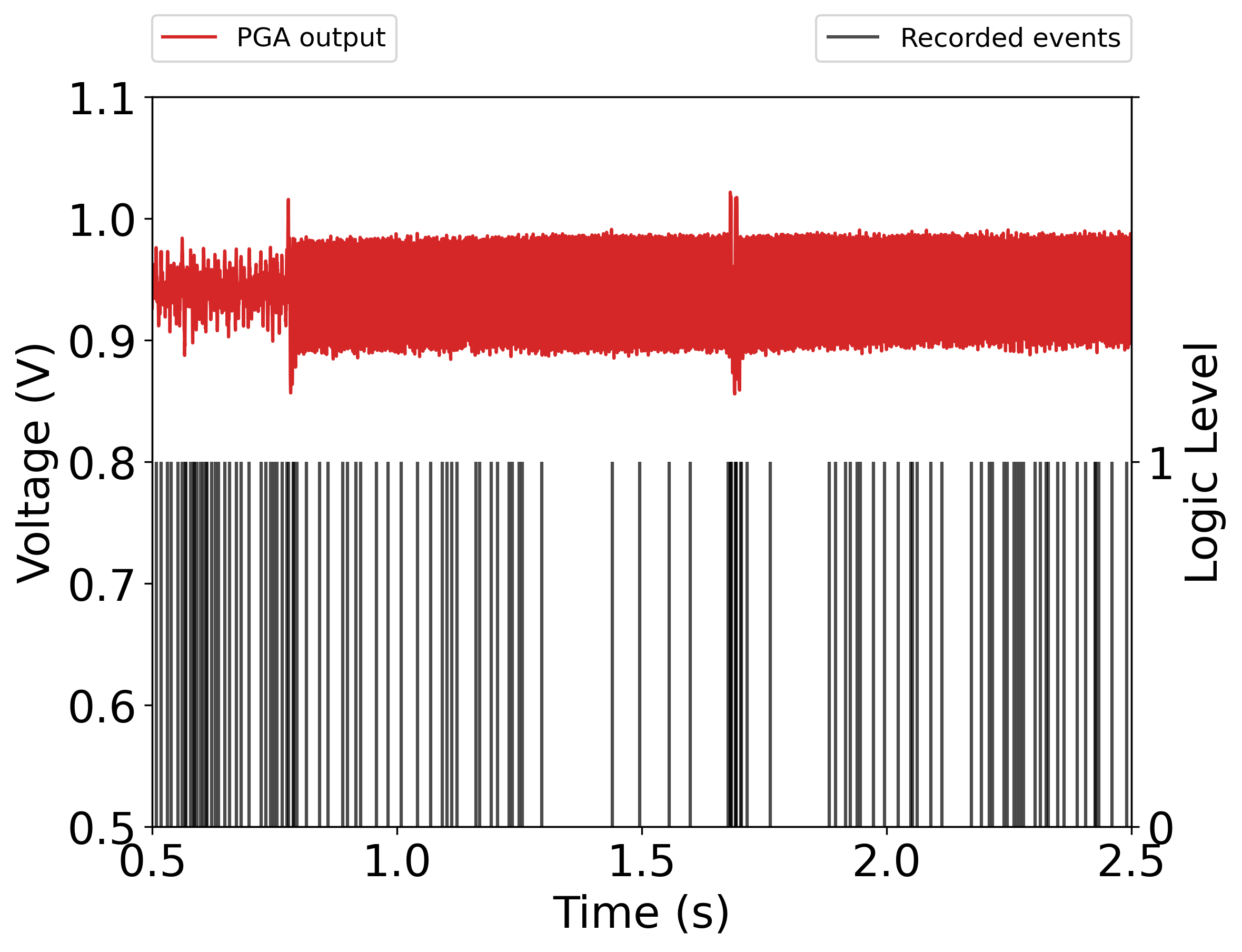
Figure 8 shows experimental measurements of an analogous experiment run directly on the ASIC. The synthetic control stimulus was scaled appropriately to \(20\) mV amplitude and played into the chip. In order to match the silicon measurement with simulation, just one channel was enabled with the rest of the channels disabled. The voltage shown in Fig. 8 is a real oscilloscope capture of the PGA output signal. The events of the aADM were recorded at the output in form of the AER with external handshaking hardware in the loop. The chip recorded data demonstrates adaptation in the recorded events while encoding the event of interest near \(t=1.7\) s, validating the hardware implementation of the adaptive event-encoding circuit.
4 Conclusions↩︎
We successfully demonstrated the operation of an event-based analog front-end ASIC with 32 parallel channels, featuring extensive programmability via SPI, and supporting the AER output protocol commonly used by neuromorphic SNN processors. By implementing an aADM encoder alongside a standard PFM encoder, the ASIC resolves the critical issue of data saturation in long-term sensor monitoring [25] while providing sensor-level tunable and adaptive data compression features for a wide variety of Brain-Computer Interface applications. This architectural breakthrough positions the ASIC as a versatile companion front-end for interfacing low-frequency biomedical signals directly with asynchronous SNN processors.
Acknowledgments↩︎
We would like to thank Chenxi Wen the Institute of Neuroinformatics, University of Zurich and ETH Zurich for carrying out the circuit-level simulations of the aADM used in Fig. 7. Part of this work was supported by the Swiss National Science Foundation (SNSF projects 204651 and 217160). During the preparation of this work, the author(s) used generative AI tools to assist with language editing and revising the manuscript text, including improving sentence structure, clarity, and adherence to academic style conventions. The tool(s) was used solely to improve clarity, grammar, and readability of author-written content. The tool(s) was not used to generate original scientific content, data, analysis, or conclusions. After using this tool, the author(s) reviewed and edited the content as necessary and take(s) full responsibility for the accuracy and integrity of the final content of the article.