GPU-Accelerated Effective Resistance Analysis for 3D IC Power Delivery Network
July 07, 2026
Abstract
Three-dimensional (3D) integration is a critical technique for enhancing transistor density, improving power efficiency, and reducing interconnect delays. However, as current demands and design complexity increase, power deliver networks (PDNs) are facing growing challenges. Careful planning of through-silicon vias (TSVs) is essential for ensuring reliable PDNs, where effective resistance serves as a vital metric for the reliability. Ill-planned TSVs often cause 3D IC with unevenly distributed effective resistance and consequently severer IR Drop. In this paper, we propose a GPU-accelerated framework on accurate effective resistance analysis for early stage 3D IC PDNs. The proposed framework achieves a speedup of 5 to 6 orders of magnitude compared to the conventional direct solver, while maintaining negligible deviations in both maximum and average relative errors.
1 Introduction↩︎
As the semiconductor industry continues to push the boundaries of Moore’s Law, three-dimensional (3D) integration has emerged as a vital technology for increasing transistor density in integrated circuits (ICs). By utilizing through-silicon vias (TSVs) to vertically stack multiple dies, 3D integration provides several key advantages, such as increased bandwidth, reduced footprint, lower interconnect delay, and improved energy efficiency [1]. However, the implementation of 3D ICs introduces substantial challenges, particularly in the design and verification of power delivery networks (PDNs)[2], [3]. Unlike traditional two-dimensional (2D) ICs, where each die has an independent PDN, 3D ICs employ a shared PDN that connects multiple dies through TSVs. This shared PDN architecture significantly increases design complexity, exacerbating issues such as power supply noise (PSN) and thermal hotspots. As a result, the risk of excessive IR drop becomes a critical concern, complicating the reliable design of 3D IC PDNs[4].
In 3D ICs, maintaining stable voltage levels across all dies is critical, and this stability is heavily influenced by the placement and grouping of TSVs [5]. TSV placement is often determined early in the design process due to its implications for both packaging and manufacturing. Once fixed, these TSVs define the current paths within the PDN, making it crucial to ensure that their placement supports the reliability and performance of 3D ICs. Effective resistance plays a key role in evaluating current flow through the PDN and the distribution of voltage drops [6], [7]. Uneven resistance distribution can lead to localized IR drops that degrade performance or cause chip failure, which are difficult to resolve in later design stages. Thus, fast and accurate effective resistance analysis is crucial during the early stages of 3D IC design.
Effective resistance analysis has traditionally been approached as part of power integrity verification or PSN sign-off using standard PSN analysis methods [8]–[18]. However, most existing methods were developed for 2D PDNs and do not fully leverage the structural properties of 3D PDNs, potentially resulting in inefficient computations when applied to 3D ICs. Moreover, early-stage PDN design requires the ability to rapidly evaluate various design options [19]. As the number of stacked dies increases, the number of possible effective resistance paths from the IPs/modules on the bottom tier to the bumps on the top tier also increases exponentially, making traditional methods for analyzing effective resistance computationally expensive and slow. At the early design stage, there exist tens to hundreds of thousands of effective resistance paths from bumps, through TSVs, to the current loads (defined at IPs or modules) in 3D ICs. Although some approaches have explored parallel acceleration techniques for general PDN analysis, these methods are not optimized for effective resistance calculations, particularly for the unique structure of 3D ICs.
To address these challenges, this paper introduces an advanced GPU-accelerated framework tailored for early-stage effective resistance analysis in 3D IC PDNs. The proposed framework enhances the computation of effective resistance across various bump-load configurations by employing a divide-and-conquer strategy that partitions the 3D PDN into multiple 2D sub-networks. This decomposition not only enables efficient GPU-accelerated analysis but also significantly reduces computational complexity, thereby enhancing scalability for larger 3D IC designs. The contributions are summarized as follows:
We introduce a divide-and-conquer strategy that decomposes the 3D PDN into multiple 2D sub-problems, which can be analyzed independently and in parallel to improve the scalability.
We reformulate the original PDN system conductance matrix—initially intended for voltage drop analysis—into a specialized formulation optimized for effective resistance computation, thereby reducing the problem size.
The proposed framework is highly compatible with GPU-acceleration platforms, enabling concurrent computation of effective resistance across multiple bump-load pairs, thus further accelerating the analysis process.
The experimental results demonstrate that the proposed framework significantly outperforms the prior works in both efficiency and scalability. For large-scale 3D IC designs, our framework was able to compute effective resistances for millions of bump-load pairs in a matter of seconds, a task that would be nearly infeasible using a golden direct solver [17] or a most recently published effective resistance solver [18]. The results also highlight the scalability of the proposed framework, with runtimes that increase linearly with the total number of nodes and bump-load pairs, making it well-suited for modern 3D PDN designs. Finally, our framework allows designers to explore and optimize TSV planning, facilitating better current distribution or significant routing area saving in practical scenarios.
2 Background↩︎
2.1 Formulation of DC analysis for PDN↩︎
Power grid analysis is essential for evaluating voltage drops across nodes in the PDN. In DC analysis, the power grid is modeled as a resistive network, represented by the following linear system using modified nodal analysis (MNA): \[ GV = I\label{eq:DC95formulation}\tag{1}\] where \(G\) is the conductance matrix, \(V\) is the vector of node voltages, and \(I\) is the vector of current sources. Given that \(G\) is sparse, symmetric, and positive definite, direct solution methods typically utilize Cholesky factorization with forward/backward substitution to solve this system [17], [20]. DC analysis is routinely performed to compute the voltages of all PDN nodes, from early-stage checks to sign-off verification [17], [19].
2.2 Effective resistance of PDN↩︎
In a PDN, the effective resistance between two nodes, \(a\) and \(b\), can be defined as the absolute value of the voltage difference between them when a unit current is injected into \(a\) and extracted from \(b\), as shown in 1 [21]. Let \(G\) be a graph representing the PDN with its Laplacian matrix \(L_G\). The effective resistance between \(a\) and \(b\) is: \[\label{eq46the32general32approch32of32effr32computation} R(a,b) = (e_a - e_b)^T L_G^\dagger (e_a - e_b)\tag{2}\] where \(L_G^\dagger\) is the pseudo-inverse of \(L_G\), and \(e_a\) denotes the \(a_{th}\) column of the identity matrix. As this expression suggests, computing effective resistance in general is computationally expensive due to the matrix inversion involved.
For early stage, it is critical to find out the effective resistance from bumps to current loads for TSV or bump planning. There are a few prior works focusing on simplifying the above formulation from the definition. For example, for an early-stage 2D uniform PDN with \(M\times N\) nodes, [10] proposed to calculate the effective resistance across \((x_1, y_1)\) and \((x_2, y_2)\) as: \[\small \label{eq:effR95for95regular95grid} \begin{align} &R = \frac{r}{N}|x_1-x_2|+\frac{s}{M}|y_1-y_2|+ \frac{2}{MN}\sum_{m=1}^{M-1}\sum_{n=1}^{N-1} \\ &\frac{ [ cos(x_1 + \frac{1}{2})\theta_m cos(y_1 + \frac{1}{2})\phi_n - cos(x_2 + \frac{1}{2})\theta_m cos(y_2 + \frac{1}{2})\phi_n ]^2 }{r^{-1}(1-cos\theta_m)+s^{-1}(1-cos\phi_n)} \end{align}\tag{3}\] where \(r\) and \(s\) are the unit resistance for the horizontally- and vertically routed PDN wires, \(\theta_m=\frac{m\pi}{M}\) and \({\phi_n=\frac{n\pi}{N}}\).
With the computed effective resistance, designers can easily compute the voltage at critical nodes, which is more important at early design stage than obtaining the voltages at all nodes [14], [19]. For instance, as shown in [14], if the bump node \(n_{{bump}}\) is connected to an ideal voltage \(v_{{bump}}\) and \(n_{load}\) nodes are connected to current loads with the \(k_{th}\) load carrying \(I_{{load}(k)}\), the node voltage \(v_{j}\) at node \(n_j\) is expressed by: \[\begin{align} \label{eq:effR32based32node32voltage} v_{j}=v_{bump}-\frac{1}{2}\sum_{k=1}^{n_{load}} [I_{load(k)}\times(R_{n_{bump}, n_j}\\ +R_{n_{bump}, n_{load(k)}}-R_{n_j, n_{load(k)}})] \end{align}\tag{4}\] where \(R_{n_{bump}, n_j}\), \(R_{n_{bump}, n_{load(k)}}\), and \(R_{n_j, n_{load(k)}}\) are the effective resistances between \(n_{bump}\) and \(n_j\), \(n_{bump}\) and \(n_{load(k)}\), and \(n_j\) and \(n_{load(k)}\), respectively.
![Figure 1: Definition of effective resistance [21].](/article/2607.05818/figs/effR-definition.png "fig:")
3 Proposed Framework↩︎
3.1 Overview↩︎
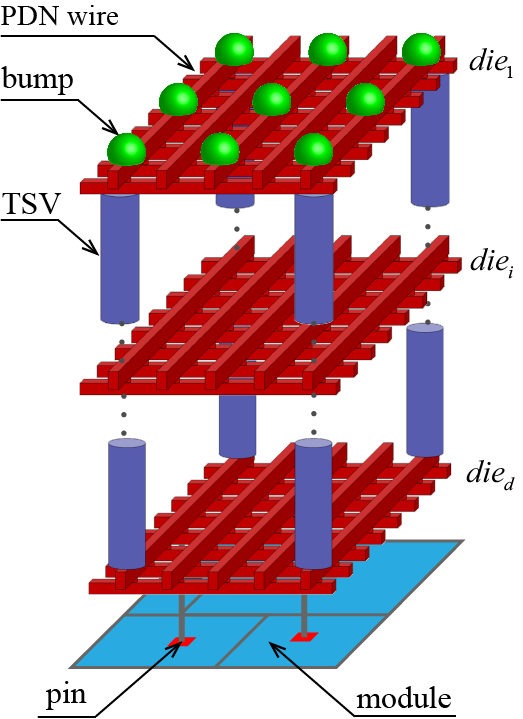
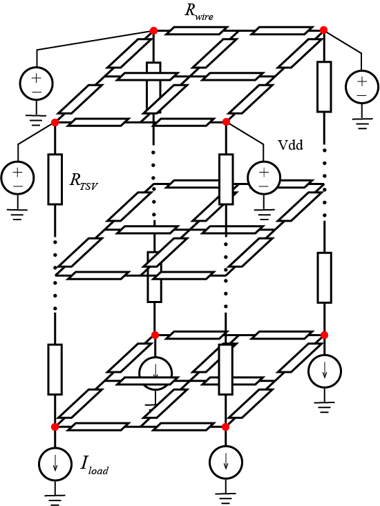
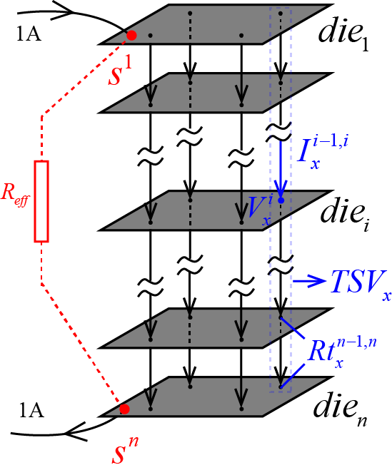
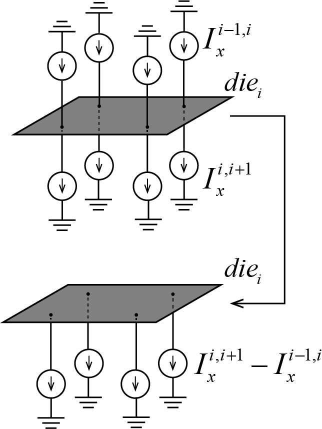
Figure 2: Key steps of the proposed framework for effective resistance analysis of 3D PDN..
In the conventional design flow, PDN is typically finalized during the placement and routing stage. Thus, at the early design stage, designers synthesize the PDN using a few critical physical parameters, such as wire width and pitch for each layer, TSV size, pitch, and density, bump pitch, and density, \(etc.\), to generate a synthetic layout, as shown in Fig. 2 (a). This layout is then extracted to build the equivalent resistor network model of the PDN (Fig. 2 (b)). Although early-stage PDNs often exhibit uniform mesh structures that can be exploited to expedite analysis, the sheer size and complexity of 3D ICs make even these simplified PDNs computationally challenging to analyze. To overcome these challenges, the proposed framework computes the effective resistance through the following:
We employ a divide-and-conquer strategy to simplify 3D PDN analysis by decomposing it into multiple 2D PDNs, each corresponding to a single die (Fig. 2 (c)). TSVs are modeled as current sources, enabling independent analysis of each 2D PDN (2 (d)).
Subsequently, the proposed framework computes the intra-die effective resistance between specified points within each 2D PDN. These intra-die results are essential for capturing the local resistive behavior within each die.
Finally, after completing the intra-die analysis, the framework calculates the inter-die effective resistances, specifically from bumps to loads.
By employing the above flow, the proposed framework is inherently well-suited for GPU acceleration, enabling rapid evaluation of various design alternatives to ensure that effective resistance is consistently balanced throughout the 3D IC.
3.2 Synthesis and Extraction↩︎
In the early stages of 3D IC PDN design, the focus is on efficiently capturing critical layout features, such as topology and bump/TSV planning, rather than replicating the final tape-out design [19]. Common assumptions for early-stage 3D IC PDN design include: (1) Bumps connected to the top-tier die are modeled as ideal independent voltage sources, while loads are modeled as ideal independent current sources; (2) The 3D IC PDN is formed by interconnecting multiple 2D PDNs using TSVs. To synthesize the PDN, synthesis algorithms generate the layout based on interconnect specifications predetermined by process technology, metal properties, and design constraints. After synthesis, the initial grid is legalized to ensure compliance with design rules regarding width and pitch. Finally, layout-dependent parasitics, such as resistance, are extracted using standard extraction flows or library-based models [19].
3.3 Effective Resistance Calculation for A Specific Bump-Load Pair↩︎
| Name | Description |
|---|---|
| \(m\) | Number of nodes connecting to voltage sources |
| \(n\) | Number of nodes connecting to current loads |
| \(d\) | Number of stacked dies |
| \(p\) | Number of TSVs |
| \(t_j^i\) | Intersection node of \(TSV_j\) and the \(i_{th}\) tier \(die_i\) |
| \(s^i\) | (Virtual) supply node of the \(i_{th}\) tier \(die_i\) |
| \(V_j^i\) | Voltage of \(t_j^i\) |
| \(V_s^i\) | Voltage of \(s^i\) |
| \(I_k^{i,i+1}\) | Inter-die TSV current between \(die_i\) and \(die_{i+1}\) for \(TSV_k\) |
| \(Rt_k^{i,i+1}\) | Inter-die resistance between \(die_i\) and \(die_{i+1}\) for \(TSV_k\) |
| \(R_{j,k}^i\) | Intra-die effective resistance between \(t_j^i\) and \(t_k^i\) |
| \(R_{s,k}^i\) | Intra-die effective resistance between \(s^i\) and \(t_k^i\) |
The most accurate method to compute the effective resistance between a bump and a load in a 3D IC is to inject a unit current (e.g., 1A) and measure the resulting voltage difference between the two nodes, as illustrated in 2 (c). This voltage difference directly represents the effective resistance. However, computing this for a 3D IC involves solving for the voltages of all nodes, making it computationally expensive to evaluate effective resistances for all bump-load combinations.
To facilitate the analysis, a few notations are introduced in Table [tbl:tab:notation]. While the actual bumps are placed on the top tier, we can still designate a supply node \(s^i\) on the \(i_{th}\) tier \({die}_i\). For a given bump-load pair, let bump and load nodes be \(s^1\) and \(s^d\), respectively. The effective resistance can then be expressed as: \[\label{eq:sum95of95vol95diff} R = V_s^1 - V_s^d = \sum_{i=1}^{d-1} (V_s^i - V_s^{i+1}).\qquad{(1)}\] This indicates that the effective resistance of a bump-load pair in a 3D PDN can be decomposed into several components, each corresponding to the voltage difference between the supply nodes of two adjacent dies, \({i.e.}\), \(V_s^i - V_s^{i+1}\).
Based on Sec. 2, the voltage at any intersection node \(t^i_j\) between the \(j_{th}\) TSV and the \(i_{th}\) die can be derived using Eq. 4 1. \[\label{eq:die95i95application} V_j^i = V_s^i - \frac{1}{2}\sum_{k=1}^p (I^{i,i+1}_k - I^{i-1,i}_k)(R_{s,j}^i + R_{s,k}^i - R_{j,k}^i),\tag{5}\] where \(j = 1, 2, \dots, p\) for \(p\) TSVs. Since the voltages at the intersection nodes of a TSV (i.e., the endpoints of a TSV segment) between two tiers must obey Ohm’s law, \(V_j^i - V_j^{i+1} = I_j^{i,i+1} R_t^{i,i+1}\), we can subtract the expression for \({die}_{i+1}\) from that for \({die}_i\), for \(i = 1, 2, \dots, d-1\): \[\label{eq:seqential95subtration} \begin{align} I_j^{i,i+1}Rt_j^{i,i+1} & = (V_s^i - V_s^{i+1}) - \sum_{k=1}^{p} I_k^{i,i+1}(a^i_{s,j,k} + a^{i+1}_{s,j,k}) \\ & + \sum_{k=1}^p I_k^{i-1,i} a^i_{s,j,k} + \sum_{k=1}^p I_k^{i+1,i+2} a^{i+1}_{s,j,k}, \end{align}\tag{6}\] where \(j = 1, 2, \dots, p\) and \(a_{s,j,k}^i=(R_{s,j}^i + R_{s,k}^i - R_{j,k}^i)/2\). In Eq. 6 , only the voltage difference \(V_s^i - V_s^{i+1}\) and the inter-die TSV currents \(I_j^{i,i+1}\) are unknown, since \(a_{s,j,k}^i\) can be easily computed using Eq. 3 . In addition, as previously assumed, a unit current is injected for effective resistance computation. Thus, the following condition always holds for inter-die TSV currents at different tiers: \[\label{eq:sum95of95segment95current} \sum_{j=1}^p I_j^{i,i+1} = 1,\quad\quad i = 1, 2, \dots, d-1.\tag{7}\]
With the above derivations, Eq. 6 and 7 can be further rewritten in matrix form: \[\label{eq:reduced95matrix95form} \begin{bmatrix} A + D & B \\ B^T & \mathbf{0} \end{bmatrix} \begin{bmatrix} \mathbf{I} \\ \mathbf{V} \end{bmatrix} = \begin{bmatrix} \mathbf{0} \\ \mathbf{1} \end{bmatrix},\tag{8}\] where the sub-matrices \(A\), \(B\) and \(D\) are: \[A = \begin{bmatrix} \begin{smallmatrix} A^1 + A^2 & -A^2 & \mathbf{0} & \ldots & \mathbf{0} \\ -A^2 & A^2 + A^3 & -A^3 & \ldots & \mathbf{0} \\ \mathbf{0} & -A^3 & A^3 + A^4 & \ldots & \mathbf{0} \\ \vdots & \vdots & \vdots & \ddots & \vdots \\ \mathbf{0} & \mathbf{0} & \mathbf{0} & \ldots & A^{d-1} + A^d \end{smallmatrix} \end{bmatrix},\]
\[B = \begin{bmatrix} \mathbf{1}_p & \ldots & \mathbf{0} \\ \vdots & \ddots & \vdots \\ \mathbf{0} & \ldots & \mathbf{1}_p \end{bmatrix},\] \[D = diag([Rt_1^{1,2}, \dots, Rt_p^{1,2}, \dots, Rt_1^{d-1,d}, \dots, Rt_p^{d-1,d}]),\] \[A^i = \begin{bmatrix} a^i_{s,1,1} & \ldots & a^i_{s,1,p} \\ \vdots & \ddots & \vdots \\ a^i_{s,p,1} & \ldots & a^i_{s,p,p} \end{bmatrix},\] and \(diag(.)\) converts a vector to a diagonal matrix. \(\mathbf{1}_p\) is an \(p\)-dimensional column vector of ones. \(\mathbf{I}\) and \(\mathbf{V}\) are: \[\mathbf{I} = \begin{bmatrix} I_1^{1,2} & \ldots & I_p^{1,2} & \ldots & I_1^{d-1,d} & \ldots & I_p^{d-1,d} \end{bmatrix}^T,\] \[\label{eq:v95expression} \mathbf{V} = \begin{bmatrix} -(V_s^1 - V_s^2) & \ldots & -(V_s^{d-1} - V_s^d) \end{bmatrix}^T.\tag{9}\]
Thus, the effective resistance for a particular bump/load pair can be rigorously obtained using Eqs. ?? and 8 9 . It is noted that the dimension of the coefficient matrix in Eq. 8 is \((p+1) \times (d-1)\), approximately corresponding to the number of TSVs multiplied by the number of dies, which is significantly smaller than the system conductance matrix that must be solved in the traditional method, with dimensions equivalent to the total number of nodes.
3.4 Fast Computation of Effective Resistances for Arbitrary Bump-Load Combinations↩︎
Eq. 8 defines the relationship between intra-die and inter-die effective resistance for a specific bump-load pair. However, a major challenge arises: changing either the bump or load node requires recomputing the coefficient matrix, \([A + D \quad B; B^T \quad 0]\), in Eq. 8 . This significantly impedes the efficient computation of effective resistances across numerous bump-load pairs, as the matrix decomposition cannot be reused. The root cause is the dependency on terms like \(R_{s,j}^i\), which vary with the specific bump and load nodes.
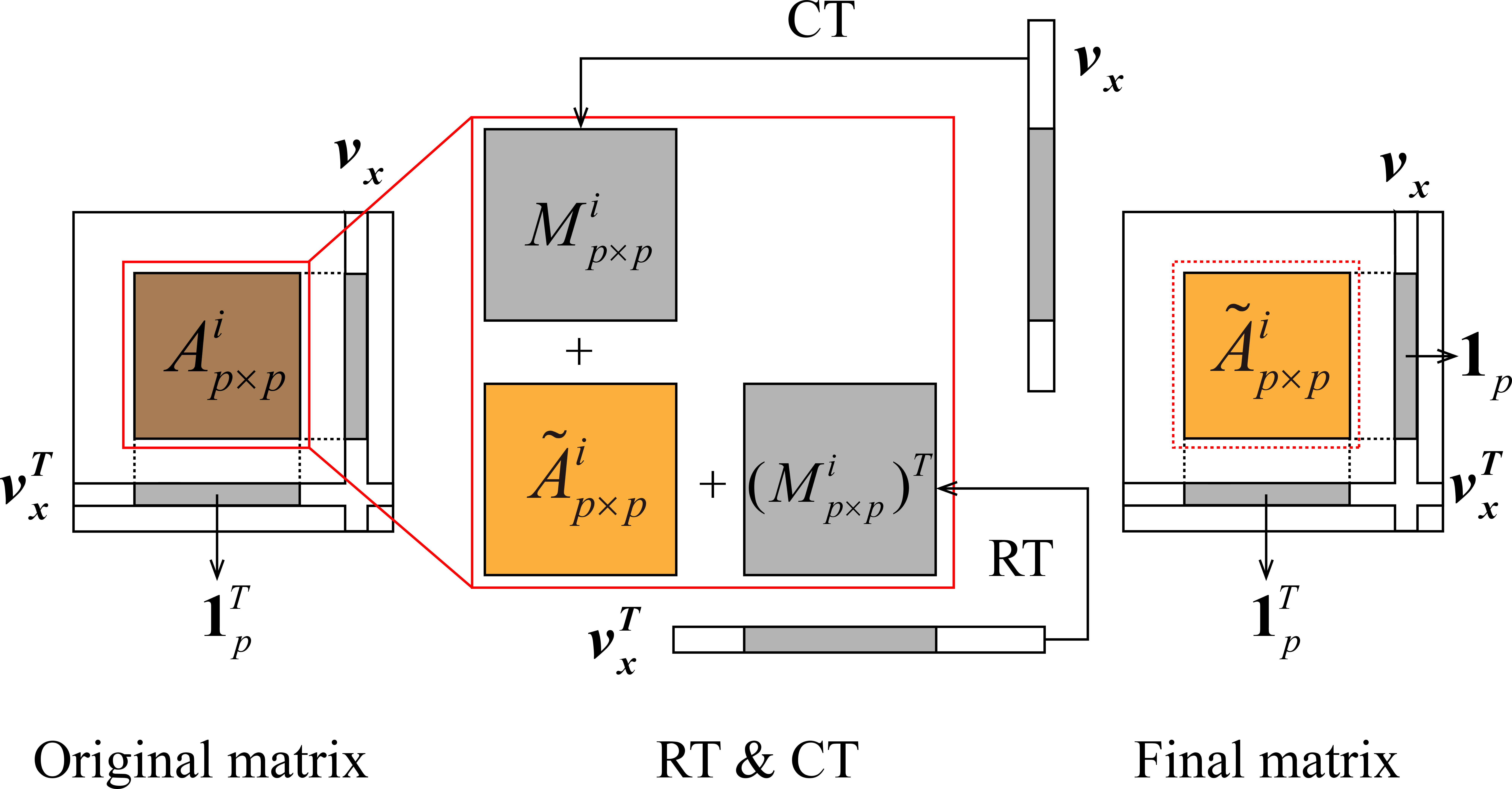
To address this, we apply row and column transformations to the matrix, eliminating dependencies on specific bump-load combinations and producing a reusable coefficient matrix for effective resistance computation. Specifically, the matrix \(A^i\) can be expressed as the sum of three components: \(\tilde{A}^i + M^i + (M^i)^T\), where \[M^i = \begin{bmatrix} R_{s,1}^i\mathbf{1}_p & R_{s,2}^i\mathbf{1}_p & \ldots & R_{s,p}^i\mathbf{1}_p \end{bmatrix},\] \[\tilde{A}^i=-\frac{1}{2} \begin{bmatrix} 0 & R^i_{1,2} & \ldots & R^i_{1,p} \\ R^i_{2,1} & 0 & \ldots & R^i_{2,p} \\ \vdots & \vdots & \ddots & \vdots\\ R^i_{p,1} & R^i_{p,2} & \ldots & 0 \\ \end{bmatrix}.\] Importantly, only \(\tilde{A}^i\) is independent of the bump-load combination. For each \(A^i\), we can identify a column \(v_x\) and a row \(v_x^T\) that align with \(\mathbf{1}_p\), as shown in 3. By performing row transformations (RTs) and column transformations (CTs), we effectively eliminate the contributions of \(M^i\) and \((M^i)^T\), resulting in a simplified and reusable coefficient matrix.
Due to the symmetry of the problem, these transformations are applied symmetrically. After the transformations, the structure of the linear system in Eq. 8 is modified, particularly altering the solution vector. The transformed system can be expressed as: \[\label{eq:matrix95transformed} \begin{bmatrix} \tilde{A}+D & B \\ B^T & \mathbf{0} \end{bmatrix} \begin{bmatrix} \mathbf{I} \\ \mathbf{\tilde{V}} \\ \end{bmatrix} = \mathbf{b},\tag{10}\] where \(\mathbf{b}\) is: \[\begin{bmatrix} \begin{smallmatrix} -\frac{1}{2}R_{s,1}^1 & \ldots & -\frac{1}{2}R_{s,p}^1 & \mathbf{0} & -\frac{1}{2}R_{s,1}^{d} & \ldots & -\frac{1}{2}R_{s,p}^d & \mathbf{1}_{p}^T \end{smallmatrix} \end{bmatrix}^T;\] \(\mathbf{\tilde{V}}\) is a vector of \(\tilde{v}_i\) with its \(i_{th}\) component as: \[\begin{align} \tilde{v}_i = &-(V_s^{i}-V_s^{i+1})+\sum_{j=1}^{d-1}({R_{s,j}^i+R_{s,j}^{i+1}})I_j^{i,i+1}\\ &-\sum_{j=1}^{d-1}{R_{s,j}^iI_j^{i-1,i}-\sum_{j=1}^{d-1}R_{s,j}^{i+1}}I_j^{i+1,i+2}. \end{align}\] Similarly, we can define \(R_{s,j}^{0}\) and \(R_{s,j}^{d+1}\) as zero, and \(\tilde{A}\) is analogous to \(A\) but with \(A^i\) replaced by \(\tilde{A}^i\):
Eq. 10 can be written as \(C\mathbf{x} = \mathbf{b}\), where the target effective resistance \(R_{eff}\) is elegantly expressed as \(R_{eff} = -\mathbf{x}^T\mathbf{b}\). Importantly, the coefficient matrix \(C\) is independent of the specific bump and load nodes, depending only on geometric and physical parameters of 3D IC. This property ensures a unique coefficient matrix, requiring only one decomposition.
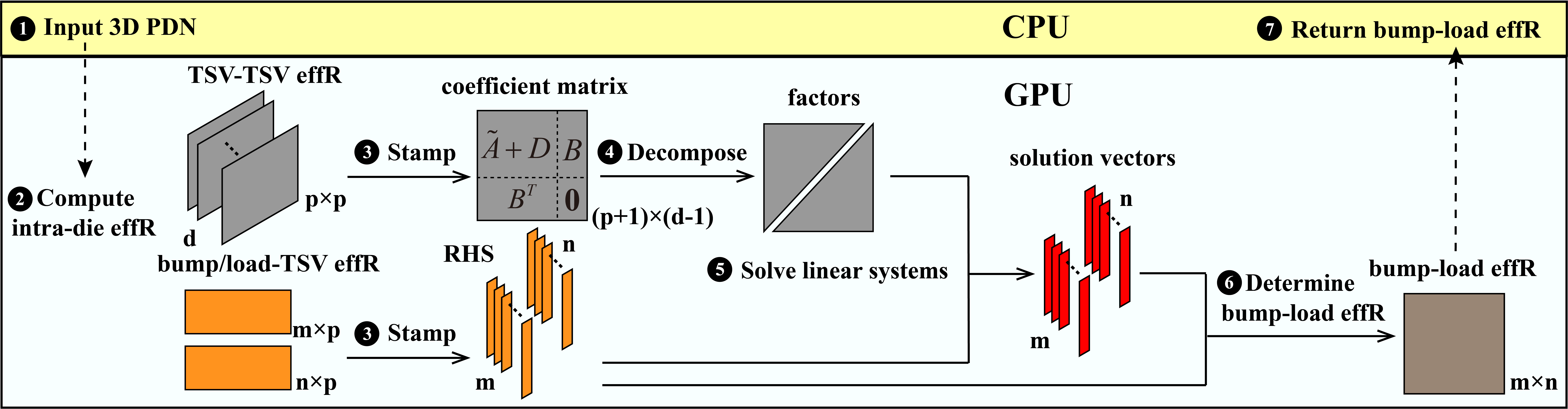
For \(m\) bump nodes and \(n\) load nodes, there are \(m \times n\) bump-load combinations, which would normally require solving \(m \times n\) linear systems based on Eq. 10 . However, leveraging the linearity of the system, this number is reduced to \(m + n\), as the vector \(\mathbf{b}\) can be split into two components: \[\label{b95partition} \begin{align} \mathbf{b}= &-\frac{1}{2} \begin{bmatrix} R_{s,1}^1 & \ldots & R_{s,p}^1 & \mathbf{0} & -\mathbf{1}_p^T \end{bmatrix}^T \\ &-\frac{1}{2} \begin{bmatrix} \mathbf{0} & R_{s,1}^{d} & \ldots & R_{s,p}^d & -\mathbf{1}_p^T \end{bmatrix}^T. \end{align}\tag{11}\] Let \(\mathbf{b} = \mathbf{b}^1 + \mathbf{b}^d\), where \(\mathbf{b}^1\) and \(\mathbf{b}^d\) depend only on the endpoints in \(\text{die}_1\) and \(\text{die}_d\), respectively. For \(m\) bump nodes in \(\text{die}_1\) and \(n\) load nodes in \(\text{die}_d\), their corresponding vectors are \(\mathbf{b}_i^1\) (\(i = 1, 2, \dots, m\)) and \(\mathbf{b}_j^d\) (\(j = 1, 2, \dots, n\)).
Taking these vectors as constants and \(C\) as the coefficient matrix, we can solve \(m + n\) linear systems, yielding solution vectors \(\mathbf{x}_i^1\) (\(i = 1, 2, \dots, m\)) and \(\mathbf{x}_j^d\) (\(j = 1, 2, \dots, n\)). The effective resistance between the \(i\)-th bump in \({die}_1\) and the \(j\)-th load in \({die}_d\) is then computed as: \[\label{eq:partition32of32solution} R_{eff}(i,j)=-(\mathbf{x}^1_i+\mathbf{x}^d_j)^T(\mathbf{b}^1_i+\mathbf{b}^d_j).\tag{12}\]
In summary, to compute \(m \times n\) effective resistances between bump and load nodes, we solve \(m + n\) linear systems using a small coefficient matrix with a size proportional to the number of dies and TSVs. Constructing these systems requires intra-die effective resistance and TSV segment resistance, both amenable to parallel computation, as shown in Eq. 3 . After decomposing the coefficient matrix, all \(m + n\) systems can be solved simultaneously, with matrix operations like dot products and additions significantly accelerated. Advanced parallel computing platforms further enhance the framework’s efficiency.
3.5 GPU Acceleration↩︎
While GPUs provide immense parallel computing capabilities with significant potential for effective resistance computation, achieving tangible performance improvements requires a comprehensive GPU-oriented redesign [22]. The proposed framework is specifically engineered to leverage this principle, as summarized in 4. In 4, TSV-TSV effective resistances (effR) represent the resistances between TSV nodes and are stored in a 3D array of dimensions \(d \times p \times p\). Bump-TSV and Load-TSV effective resistances are stored in two separate arrays of dimensions \(m \times p\) and \(n \times p\), respectively. These arrays collectively contain all required intra-die effective resistances and are used to construct the unique coefficient matrix and constant vectors. After the coefficient matrix is decomposed, solution vectors are computed using substitution. The bump-load effective resistances are then calculated using vector addition and dot products, utilizing both the constant and solution vectors. The results are organized into an array of dimensions \(m \times n\) and transferred back to the CPU host.
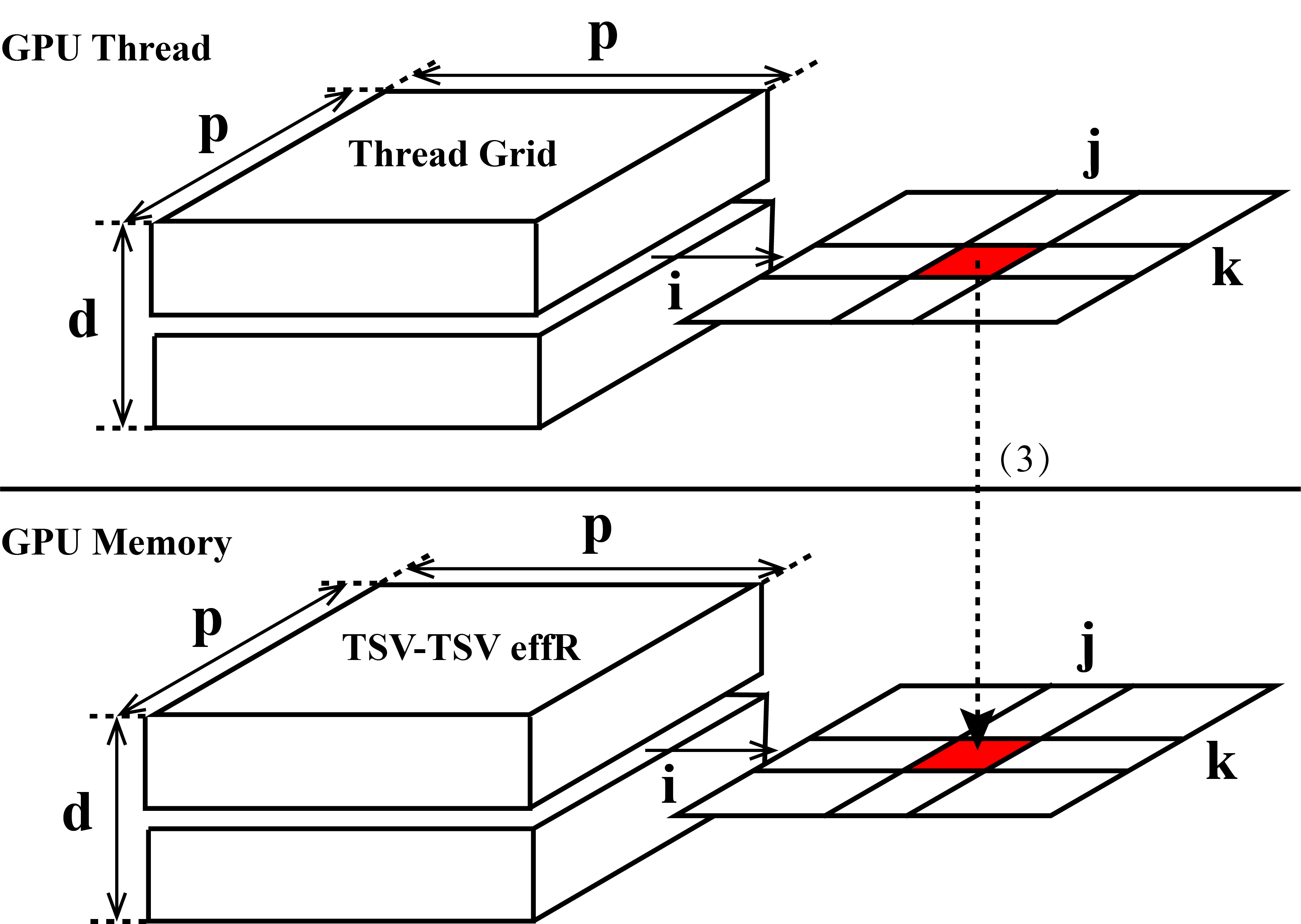
As shown in 4, the GPU handles the bulk of the computation, while the CPU manages input and output tasks. This division of labor maximizes the GPU’s parallel processing capabilities while minimizing data transfer overhead between the CPU and GPU. To further optimize performance, we reformulate Eq. 3 and refine the GPU thread configuration to avoid redundant computations and reduce floating-point operations. For thread allocation, taking the computation of TSV-TSV effective resistances as an example (illustrated in 5), a straightforward scheme is to allocate \(d \times p \times p\) threads. Each thread, indexed by \((i, j, k)\), computes the effective resistance \(R_{j,k}^i\) between the \(j_{th}\) and \(k_{th}\) TSV nodes within \({die}_i\) using Eq. 3 . The results are stored in a GPU array of size \(d \times p \times p\). However, since \(R_{j,k}^i = R_{k,j}^i\), allocating \(p \times p\) threads is unnecessary. Instead, only \(p \times (p-1)/2\) threads are needed, as the results of threads indexed by \((i, j, k)\) and \((i, k, j)\) are identical, which reduces redundant thread execution.
Additionally, directly computing intra-die effective resistance using Eq. 3 introduces significant redundancy. To alleviate the GPU’s computational burden, we partition Eq. 3 into several smaller components. Each component is computed in parallel on the GPU, and the partial results are summed up afterward.
Finally, to further optimize performance, a recursive form of the multiple-angle formula is employed for the cosine terms in Eq. 3 . This approach minimizes the use of expensive cosine operations on the GPU, replacing them with multiplication operations, which require significantly fewer floating-point computations. Since many operations in 4 are matrix-centric, established GPU-accelerated libraries such as CuPy [23] can be utilized to improve the implementation efficiency.
4 Experimental Results↩︎
| Design | #Die | Footprint (\(mm^2\)) | #Nodes | #TSV | #Bump | #Load | Runtime (sec.) | Speedup | ARE | MRE | ||
| Golden [17] | Pseudo [18] | Ours | ||||||||||
| D1 | 4 | 5.5\(\times\)7.3 | 4.4e6 | 1.8e4 | 432 | 1e4 | 3.4e6 | 31.0 | 13.3 | 2.6e5X\2.3X | 5.0e-9 | 5.1e-9 |
| D2 | 5 | 5.5\(\times\)7.3 | 5.5e6 | 2.2e4 | 432 | 1e4 | 4.3e6 | 38.7 | 14.1 | 3.0e5X\2.7X | 5.6e-9 | 5.7e-9 |
| D3 | 6 | 5.5\(\times\)7.3 | 6.6e6 | 2.7e4 | 432 | 1e4 | 5.6e6 | 46.6 | 15.1 | 3.7e5X\3.1X | 6.1e-9 | 6.2e-9 |
| D4 | 4 | 7.8\(\times\)11.9 | 1.0e7 | 2.2e4 | 1040 | 1e4 | 2.2e7 | 72.5 | 17.1 | 1.3e6X\4.2X | 8.2e-9 | 8.3e-9 |
| D5 | 5 | 7.8\(\times\)11.9 | 1.3e7 | 2.8e4 | 1040 | 1e4 | 2.8e7 | 95.0 | 18.9 | 1.5e6X\5.0X | 8.2e-9 | 8.2e-9 |
| D6 | 6 | 7.8\(\times\)11.9 | 1.5e7 | 3.4e4 | 1040 | 1e4 | 3.4e7 | 110.3 | 20.8 | 1.6e6X\5.3X | 8.8e-9 | 8.9e-9 |
| D7 | 4 | 11.0\(\times\)11.0 | 1.3e7 | 2.6e4 | 1369 | 1e4 | 4.1e7 | 103.2 | 25.8 | 1.6e6X\4.0X | 9.4e-08 | 9.5e-08 |
| D8 | 5 | 11.0\(\times\)11.0 | 1.7e7 | 3.3e4 | 1369 | 1e4 | 4.9e7 | 126.3 | 28.5 | 1.7e6X\4.4X | 1.7e-08 | 1.8e-08 |
| D9 | 6 | 11.0\(\times\)11.0 | 2.0e7 | 4.0e4 | 1369 | 1e4 | NA | 149.6 | 31.5 | NA\4.7X | NA | NA |
All experiments are conducted on an Ubuntu 22.04 host with an Intel Xeon Platinum 8475B (48 cores, 503 GB RAM) and an NVIDIA A100 GPU (80 GB). In addition to a most recent pseudo-inverse-based solver [18], a conventional CHOLMOD-based direct solver [17] is used as the golden reference.
4.1 Evaluation of Accuracy and Speed↩︎
1 summarizes the parameters of 9 early-stage 3D IC industrial benchmarks based on 14nm technology [24]–[26]. Columns 2-7 detail the number of dies (#Die), footprint (\(mm^2\)), number of PDN nodes (#Node), TSVs (#TSV), bumps (#Bump), and loads (#Load). For early-stage design, bumps and TSVs are assumed to be uniformly distributed. Columns 8-10 show the runtime for the golden solver [17]2, the pseudo-inverse-based solver [18]3, and the proposed framework.
Both solvers in [17], [18] are serial, with runtimes proportional to the number of bump-load pairs. The pseudo-inverse-based solver [18] achieves speedups at the cost of accuracy, while the proposed framework is unaffected by bump and TSV topology, delivering 5-6 orders of magnitude speedup over the golden solver and 2-5\(\times\) speedup over [18], as shown in Column 11. The last two columns list the average and maximum relative errors (denoted as ARE and MRE) compared to the golden solver [17], which are around the orders of \(10^{-9}\)-\(10^{-8}\) and hence negligible. Thus, unlike the prior works [17], [18], the proposed framework achieves both high accuracy and speed.
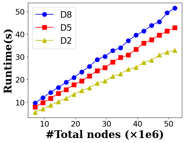
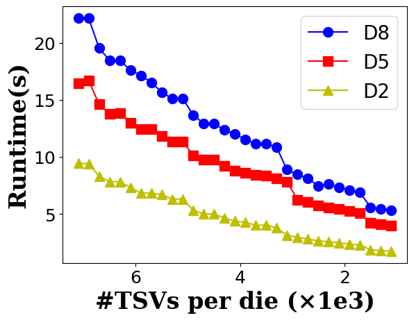

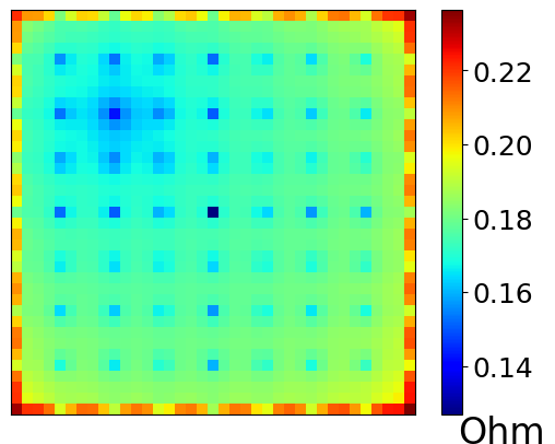
Figure 6: Comparison of (a) runtime v.s. #Node; (b) runtime v.s. #TSVs/Die; (c) runtime v.s. #Bump-load pairs for cases D2, D5 and D7; (d) Contour of effective resistance distribution..
To evaluate the scalability of our framework, we selected three key parameters, the total number of nodes, the number of TSVs per die, and the number of bump-load pairs, and then varied each parameter using ‘D2,’ ‘D5,’ and ‘D8’ as baselines while keeping all other parameters constant. The relationships between runtime and these parameters are summarized in 6 (a) 6 (b) 6 (c). It is worth noting that while the runtime increases linearly with those key parameters, the growth rate of the runtime is significantly smaller compared to the growth rate of these parameters. This again demonstrates the efficiency and scalability of the proposed framework in handling large-scale 3D PDN benchmarks.
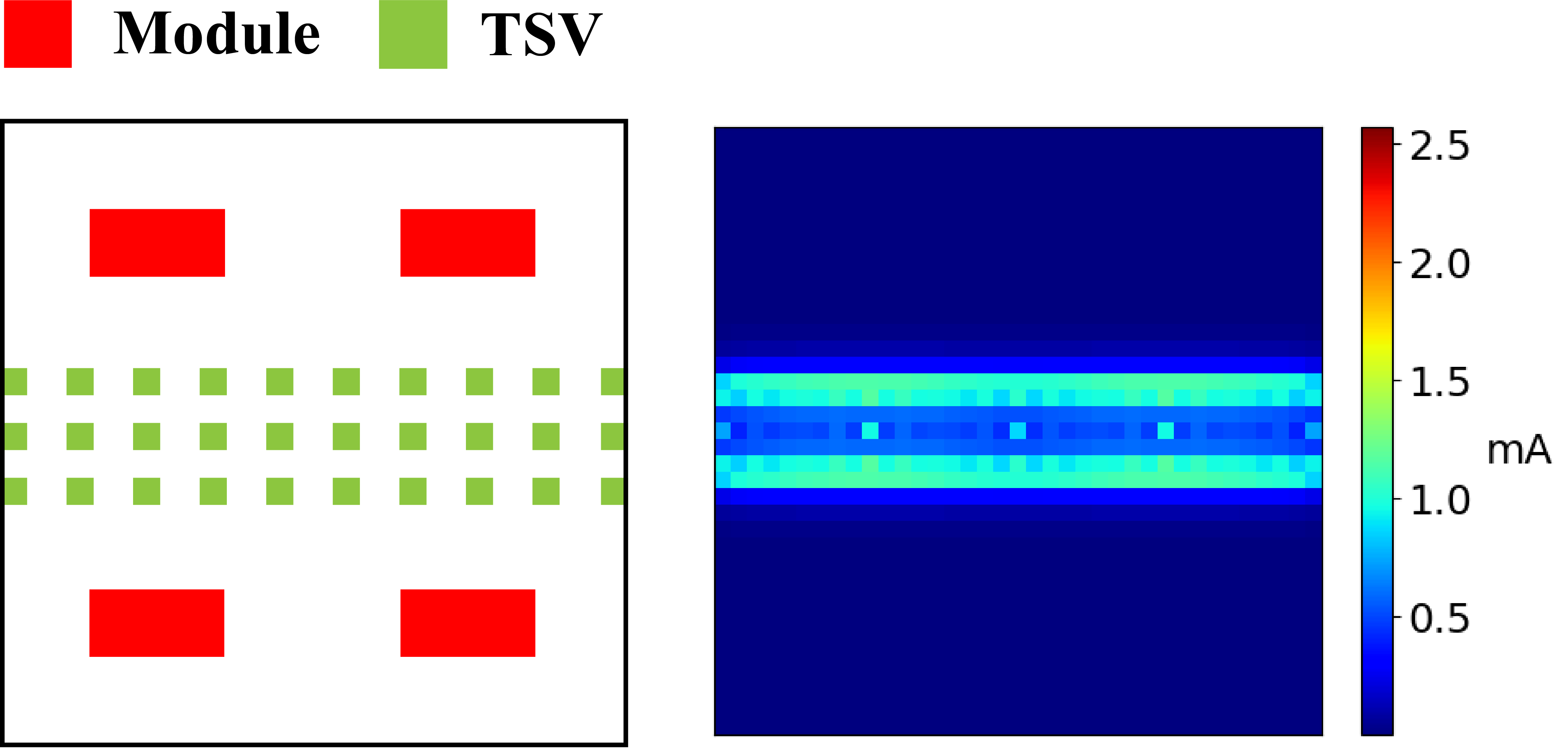
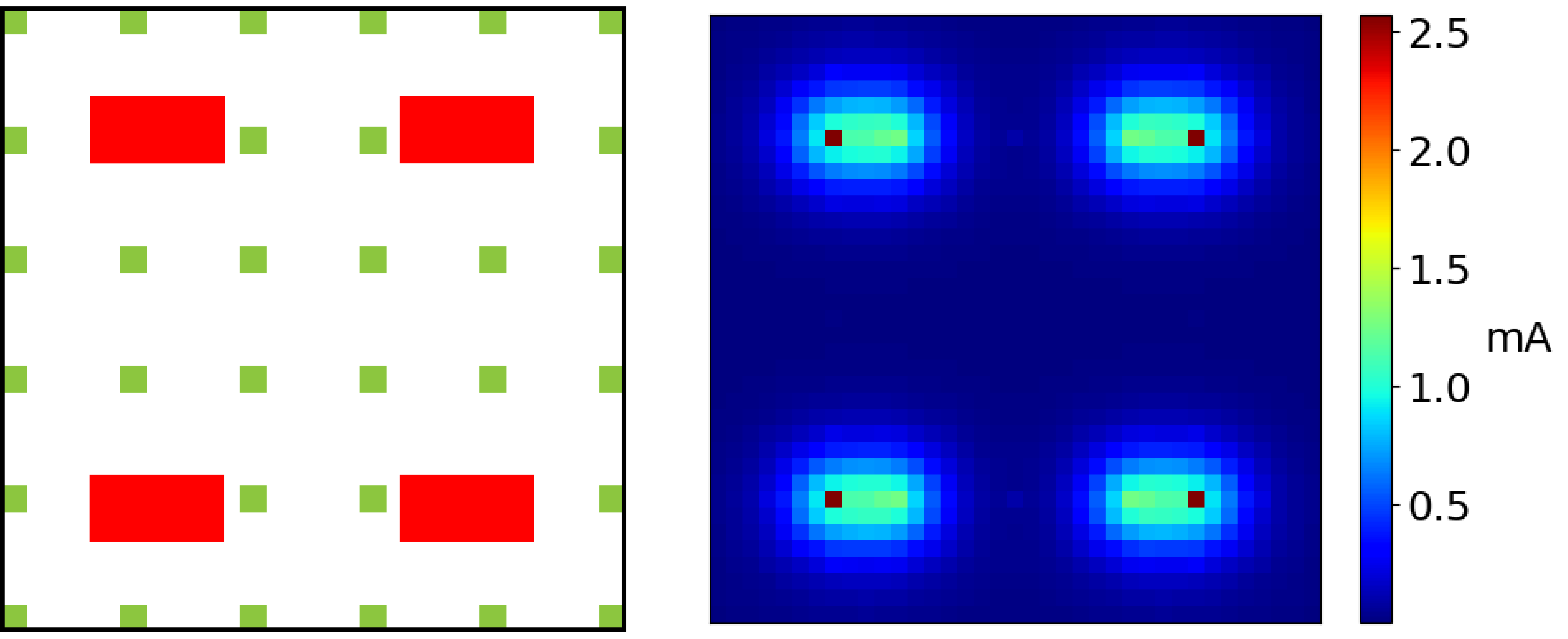
Figure 7: Through-bump current distributions for different TSV planning options: (a) Band-like placement; (b) Uniformly-distributed placement..
4.2 TSV Planning Using the Proposed Framework↩︎
The proposed framework can be readily used to facilitate evaluations of different design options at the early design stage. For example, designers can examine the contour of the effective resistance distribution in 6 (d) to select the most suitable TSV planning option. 7 (a) and (b) illustrate the impact of different TSV planning strategies, both of which are based on practical design guidelines. 7 (a) (left) places all TSVs in a centrally clustered configuration to enable a band-like connection, a setup commonly used in mainstream HBM products, whereas 7 (b) (left) distributes TSVs uniformly across the entire die to facilitate better current and thermal distribution. The through-bump currents are demonstrated and compared for the two scenarios. For the same four functional blocks, each occupying \(2.35\times1.18 mm^2\) with a current density of \(220 A/cm^2\), the band-like connection in 7 (a) results in 23.4% of the total bumps carrying approximately 95% of the total current, while also contributing to significant routing area savings. In contrast, the uniformly distributed connection in 7 (b) results in 53.2% of the total bumps carrying 95% of the total current. These insights allow designers to make informed trade-offs between different application scenarios to select the optimal TSV planning strategy.
5 Conclusion↩︎
The proposed framework presents a highly efficient and scalable solution for effective resistance analysis in the early design stages of 3D IC PDNs. By leveraging the parallel processing capabilities of GPUs, the method achieves substantial speedup compared to traditional approaches, making it feasible to handle large-scale 3D PDN designs with millions to billions of nodes. The results show that our approach not only provides fast and accurate resistance computation but also facilitates efficient design options exploration in 3D IC development.