Ten-Four: An Open-Source Fused Dot Product Unit for Mixed-Precision GPGPU Tensor Cores
November 19, 2025
Abstract
Efficient mixed-precision MMA operations are critical for accelerating deep learning workloads on GPGPUs. However, existing open-source Tensor Core implementations rely on discrete arithmetic unit designs, leading to high latency, accumulated rounding errors, and poor resource utilization. To address these challenges, we propose Ten-Four, a configurable mixed-precision fused dot product unit integrating both floating-point and integer arithmetic pipelines within a unified architecture, implemented as part of the open-source RISC-V-based Vortex GPGPU’s Tensor Core Unit extension. It supports low-precision multiplication in TF32/FP16/BF16/FP8/BF8/INT8/INT4 with higher-precision FP32/INT32 accumulation, native Microscaling (MX) support, and sparse lane clock-gating for dynamic power reduction, while matching NVIDIA Tensor Core numerical accuracy. Ten-Four achieves 4-cycle latency at 300 MHz \(F_{\text{max}}\) on the Xilinx U55C FPGA, delivering 130.368 GFLOPS peak throughput per Tensor Core and 2.7\(\times\)–7.9\(\times\) speedup over equivalent Berkeley HardFloat and FPnew based implementations at less than 60% the area cost. ASIC synthesis in 7nm FinFET achieves 2.771 TFLOPS/W peak efficiency at 1.58 GHz \(F_{\text{max}}\).
Fused Dot Product, GPGPU Microarchitecture, Mixed-Precision, Sparsity, Microscaling, Tensor Core
1 Introduction↩︎
As deep learning workloads grow in scale and prevalence, General Matrix Multiply (GEMM) acceleration has become a critical priority for GPU designers due to its dominant role in model execution. For instance, profiling Llama 3.1 8B on NVIDIA B200 GPUs showed that over 80% of the runtime is spent executing some variant of GEMM. To mitigate this bottleneck, GPU vendors introduced dedicated throughput-focused matrix engines, such as NVIDIA Tensor Cores [1] and AMD Matrix Cores [2], to execute specialized Warp-Matrix-Multiply-Accumulate (WMMA) and Matrix-Fused-Multiply-Add (MFMA) instructions, respectively.
Microbenchmarking these instructions has revealed key microarchitectural details of the underlying hardware [3]–[7]. Tensor Cores receive input sub-matrices A, B, and C directly from the SIMT Sub-Core
register file, perform an MxNxK matrix-multiply-accumulate, and write the resulting sub-matrix D back to the register file, much like the integer ALU, FPU, and LSU SIMD lanes they are placed alongside. By avoiding RF storage of
intermediate results, fused MMA operations substantially minimize power consumption and memory traffic. This enables greater compute density within the same die area, thereby improving the evermore critical throughput/mm\(^{2}\) and throughput/watt metrics in data-center GPUs.
While Tensor Cores in commercial GPUs have advanced remarkably in recent years (NVIDIA FP16 Tensor Core FLOPS increased eight-fold from Volta to Hopper generations [8]), the open-source GPGPU design space has lagged behind with sub-optimal prototypes delivering nominal throughput. This gap has only widened with the introduction of 2:4 structured sparsity since the Ampere generation [9], [10] and native hardware-accelerated OCP Microscaling (MX) format [11], [12] support in NVIDIA Blackwell [13] and AMD CDNA 4 [14] architectures. This is largely a consequence of open-source designs’ reliance on discrete floating-point arithmetic unit libraries, which introduce high latency, accumulated rounding errors, and poor resource utilization. For example, the Ventus GPGPU Tensor Core [15] and Virgo cluster-level systolic array matrix unit [16] utilize discrete arithmetic modules from the Berkeley HardFloat [17] library. Similarly, Nada et al. [18] use multiple FPnew [19] FMA instantiations in their prototype.
To address the lack of a high-performance Tensor Core implementation in the open-source GPGPU design space, we introduce Ten-Four, a novel configurable mixed-precision Fused Dot Product (FEDP) unit microarchitecture developed on top of
the RISC-V Vortex GPGPU’s [20] Tensor Core Unit (TCU) Extension. Vortex’s configurability at multiple levels of granularity
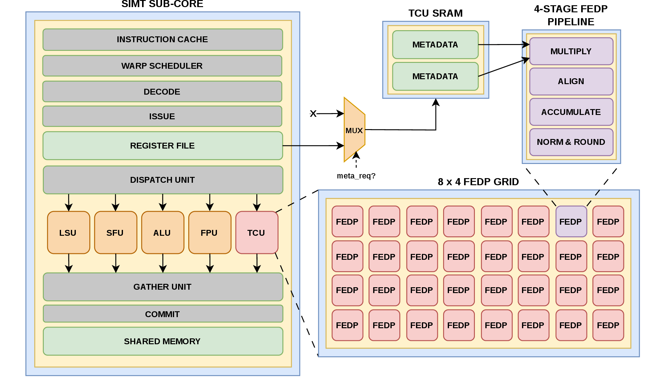
(cores, warps, threads, cache hierarchy) and mature runtime ecosystem present an ideal platform for building and evaluating our design. Fig. 1 illustrates how we adopt an [8x4] grid of 8-element FEDP
units to form a TCU within a Vortex SIMT sub-core in a 32-threads/warp configuration.
To the best of our knowledge, this is the first open-source work bridging the gap between specialized Fused Dot Product implementations and GPGPU Tensor Core prototypes. The key contributions of our work are summarized as follows:
We propose a configurable 4-cycle Fused Dot Product (FEDP) pipeline supporting low-precision multiplication in FP16, BF16, TF32, FP8(E4M3), and BF8(E5M2) with higher-precision FP32 accumulation as part of the Vortex GPGPU TCU extension.
We describe a unified pipeline methodology for integrating integer arithmetic within the floating-point datapath, incurring minimal overhead and maximizing resource reuse through a novel addend-splitting strategy.
We introduce a Sparse Lane Mask approach for reducing dynamic power consumption via clock-gating when inputs A or B are zero, thereby making inner dot product based dual-side Sparse Tensor Core designs more practical.
We support Microscaling (MX) format block-quantized inputs while preserving early addend accumulation, using a per-lane scale-factor compensation scheme.
We demonstrate 2.7\(\times\)-7.9\(\times\) speedup over equivalent Berkeley HardFloat and FPnew based implementations at less than 60% the area cost on the Xilinx U55C FPGA
ASIC synthesis using ASAP7 7nm PDK achieves 2.771 TFLOPS/W peak efficiency at 1.58 GHz \(F_{\text{max}}\), exceeding NVIDIA A100 Tensor Cores’ per-unit throughput by \(\sim\)12.3% at an iso-configuration.
2 Background and Motivation↩︎
2.1 FEDP Computation in Tensor Cores↩︎
Tensor Core WMMA instructions operate on warp-registers, which cooperatively load and store sub-matrix operands across all 32 threads of a warp. This can be conceptualized as a single 32-bit register (e.g., R0) replicated across all 32 threads, providing \(32 \times 32 = 1024\) bits of total operand capacity. To maximize data density, each thread’s 32-bit register packs two 16-bit, four 8-bit, or eight 4-bit elements.
Each MMA operand sub-tile must fit within the warp-register capacity. For FP16 inputs, a warp-register holds 1024/16=64 elements, yielding an MxK=8x8 tile for matrix A. However, since FP32 accumulation limits
matrix C to 1024/32=32 elements, we must set N=4, giving an 8x4x8 FP16/FP32 MMA shape. With FP8 inputs, the doubled packing density extends the reduction dimension, producing an 8x4x16
FP8/FP32 shape. Thus, a Tensor Core can be realized as an MxN grid of K-element FEDP unit instantiations: \[D_{m,n}^{\textit{FP32}} =
\sum_{i=0}^{K-1}
\left(A_{m,i}^{\textit{FP16}} \times B_{i,n}^{\textit{FP16}}\right)
+ C_{m,n}^{\textit{FP32}}\]
2.2 Limitations of Prior Art↩︎
Floating-point libraries. Berkeley HardFloat [17] provides IEEE 754-compliant HDL modules with configurable exponent and significand widths using a recoded intermediate representation. It has been widely adopted in open-source accelerator projects such as Gemmini [21], Virgo [16], Ventus [15], and the Chipyard SoC Framework [22]. FPnew [19] is another parameterized transprecision FPU targeting RISC-V F-extension support, with configurable formats, pipeline depths, and energy-proportional execution. It is used in the PULP Platform [23], Vortex FPU lanes [20], and Nada et al.’s Tensor Core prototype [18]. In contrast, FloPoCo [24] specifically targets FPGA arithmetic generation via parameterizable VHDL operators and automated pipelining.
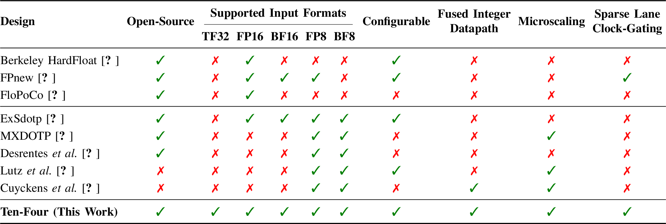
Specialized fused dot product designs. Multiple foundational works [25]–[27] address the latency, rounding, and resource penalties of composing dot products from discrete arithmetic units, incorporating features such as a shared integer datapath [28], Posit format support [29], [30], Microscaling [31]–[33], and their integration into compute clusters [34]–[37]. However, they remain narrowly scoped to specific formats or ISAs. Ten-Four bridges this gap by taking inspiration from and generalizing these fused microarchitectures into a broader, configurable, mixed-precision GPGPU Tensor Core context, as summarized in Table ¿tbl:tab:related95work?.
3 Ten-Four Microarchitecture↩︎
Ten-Four is an open-source Fused Dot Product Hardware IP 1 for developing feature-rich mixed-precision GPGPU Tensor Cores, written in SystemVerilog.
3.1 Key Arithmetic Submodules↩︎
The mixed-precision fused inner dot product datapath requires several multi-operand additions. Carry-Save Adders (CSAs) are particularly suitable for this task, as they effectively reduce N operands of W-bits each to a (W + \(\log_2\)N)-bit sum and carry without carry propagation dependencies. We develop a standard CSA using recursively chained 4:2 compressors with conditional 3:2 compressors for odd number of operands cases, alongside a MOD-4 operand grouping CSA to minimize the critical path further when seven or more operands need to be accumulated. The final summation is performed by a Kogge-Stone Adder (KSA), which outperforms carry-lookahead designs by sacrificing area efficiency to achieve lower fanout at every stage through its parallel prefix tree structure. We also implement Wallace tree multipliers (WTMUL) whose partial products are effectively reduced using CSAs. We decide against incorporating Radix-4 Booth recoding in our design, since the incurred bit-pair encoding overhead outweighed the benefit of halving partial products at our target 4-11 bit widths.
3.2 Ten-Four Mixed-Precision Floating-Point Datapath↩︎
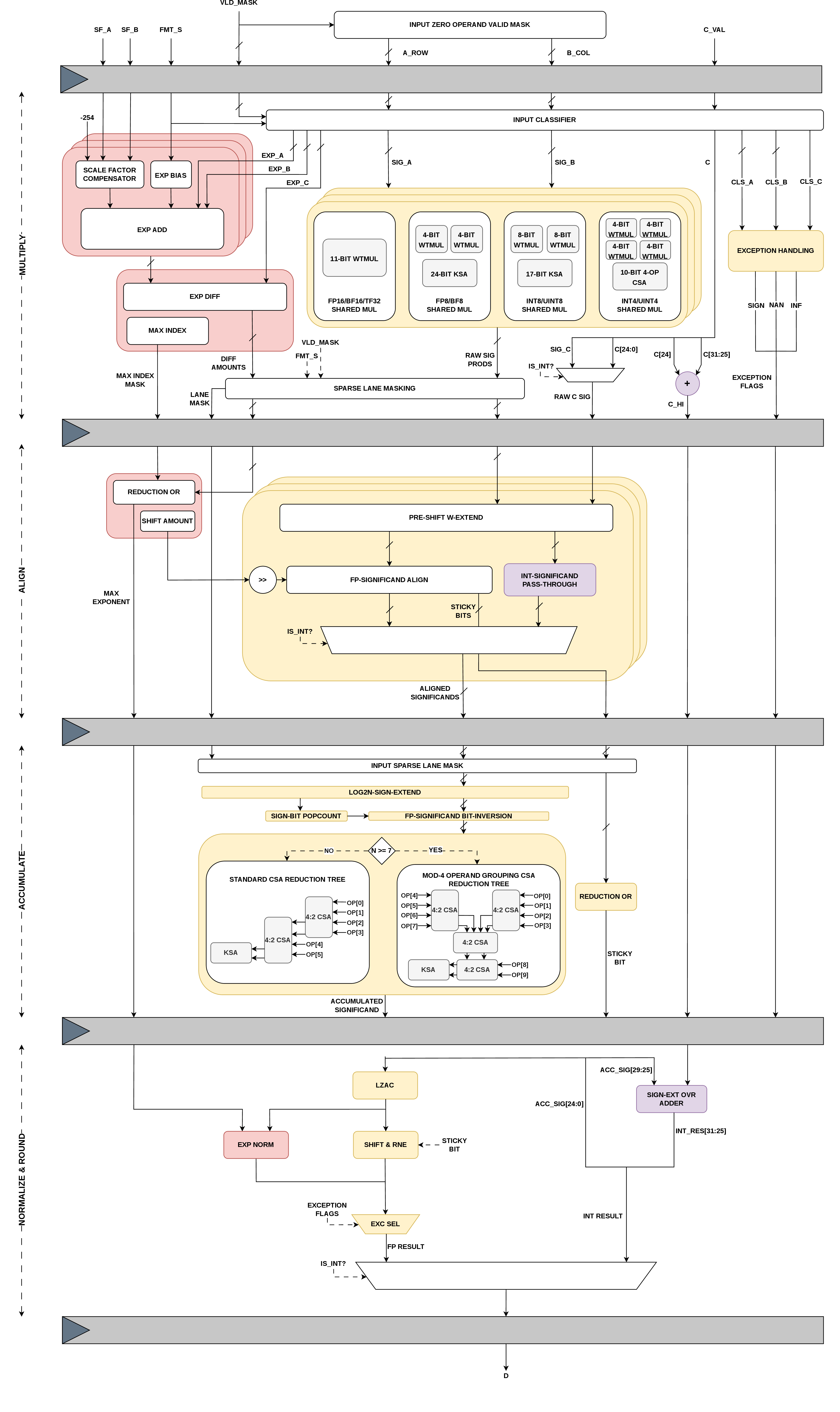
Depending on the SIMT sub-core configuration, Ten-Four performs either a four-element or eight-element FEDP at 4/8 or 16/32 threads/warp respectively. It can also be configured to selectively instantiate any subset or all of the available input formats at compile-time to reduce area and improve efficiency based on application requirements. For example, LLM training workloads that exclusively use FP16/BF16/TF32 formats can benefit from omitting the lower-precision format logic entirely. Ten-Four also obviously supports dynamic selection of the input datatype at run-time through the source format signal. As illustrated in Fig. 2, the complete Ten-Four datapath consists of 4 pipeline stages:
3.2.1 Stage-1: Shared Multiplier, Difference Matrix and Exception Handling↩︎
Ten-Four utilizes a class-wise shared multiplier scheme between formats of similar mantissa bit-widths that makes an equal tradeoff between the short critical path of format-dedicated multipliers and the area efficiency of unified sub-word partial product grids as proposed by Zhang et al. [26]. For example, all three FP16, BF16, and TF32 mantissa multiplications are performed in a single 11\(\times\)11-bit WTMUL. Accordingly, BF16 mantissas need to be zero-extended before entering the multiplier to maintain the same width. Remember that, since the inputs are packed as FP16/BF16 pairs or FP8/BF8 quads per 32-bit register, for a given K-element dot product, we instantiate 2\(\times\)K multiplier lanes in parallel. Since we can only pack one TF32 operand per 32-bit register this way, only every alternate lane is valid for this input type. In contrast, since we can pack four FP8/BF8 elements together, they require an additional reduction to maintain operand count consistency later in the pipeline. Hence, FP8 (E4M3) and BF8 (E5M2) share two 4\(\times\)4-bit WTMULs whose products are then summed with a 24-bit KSA. In this manner, all formats converge to a raw E8M25 intermediate representation to maintain consistency and efficient resource utilization in subsequent pipeline stages.
Similarly, the exponent sum of the incoming A and B operands, along with their respective format-wise FP32 bias conversions, is computed according to the equations: \[CONV_{FP16/FP32} = BIAS_{FP32} - (2\times BIAS_{FP16}) + 1\] \[EXP_{FP32} = EXP_{A} + EXP_{B} + CONV_{FP16/FP32}\]
These exponent sums are fed into the first part of our maximum exponent identification circuitry, which extends Sohn et al.’s subtractor-based comparator architecture [25] to support an arbitrary number of \(N\) operands. First, all \((N-1)\times(N-1)\) pairwise exponent differences are computed in parallel to form the difference matrix. The sign bit of each subtractor result indicates the relative magnitude of its operand pair. To reduce area overhead, we exploit symmetry by computing only the upper triangle and deriving the lower triangle by complementing the sign bits. The maximum exponent index is then extracted from the sign matrix via reduction AND and NOR logic, and passed to the next stage as a one-hot encoded mask.
Additionally, standard IEEE-754 compliant exception handling is performed in parallel to the exponent and mantissa processing. For each product, we detect NaN inputs and infinity-times-zero conditions for multiplication exceptions. Addition exceptions are detected by identifying opposing-signed infinities across the dot product elements and addend, hence producing the result’s sign, NaN, and infinity flags preemptively.
3.2.2 Stage-2: Max Exponent, Shift Amount and Significand Alignment↩︎
This stage completes the maximum exponent identification via a reduction OR on the one-hot encoded mask from the previous stage. Shift amounts are then derived by reusing the difference matrix and negating values as necessary, yielding near-\(O(1)\) critical path complexity (bounded in practice by fanout at higher \(N\)) at an \(O(N^2)\) area cost compared to traditional reduction tree comparators. Finally, the significand products are aligned using the computed shift amounts, with two extra alignment bits and per-lane sticky bits retained from the shifted-out ones to preserve precision.
3.2.3 Stage-3: Accumulation↩︎
Naive dot product implementations accumulate the addend "C" separately after dot product summation, requiring additional 2-operand alignment, normalization, and rounding that increases both rounding error and critical path delay. Our design integrates addend processing from the very first pipeline stage, where C’s exponent participates in maximum exponent finding and its significand undergoes alignment alongside product terms.
Here, the aligned significands and addend are first sign-extended to \(25 + \log_2(2K)\) bits to handle signed arithmetic correctly. Now, instead of performing a naive 2s complement on each negative term individually before the multi-operand CSA, we only bit-invert the negative significands and defer the \(+1\) correction to be collectively handled as an extra operand in the CSA, whose value is simply the total number of negative terms in the accumulation. It is calculated by performing a popcount on the sign bits of each lane. Depending on the total operand count – six for 4/8 threads/warp (\(K\) products, one addend, one correction term) or ten for 16/32 threads/warp configurations – either a standard CSA tree or a MOD-4 operand grouping CSA is selected at compile-time. Per-lane sticky bits are simultaneously reduction-OR’d into a single sticky bit for rounding the final FEDP result.
3.2.4 Stage-4: Normalization and Rounding↩︎
The final pipeline stage extracts the magnitude from the signed accumulation result and utilizes a predictive Leading Zero Counter (LZAC) for determining the normalization shift amount. The exponent is adjusted by subtracting the computed shift amount from the maximum exponent, while the mantissa is normalized by left-shifting the significand. Standard Round-to-Nearest-Even (RNE) rounding is applied using the LSB, Guard, Round, and previously extracted Sticky bit to produce the final FP32 dot product result. If an exception occurred, the result is overridden with the IEEE-compliant canonical NaN or infinity representation.
3.3 Fusing the Integer Datapath↩︎
Integer dot product operations require multiple arithmetic components already present in the floating-point datapath [28], [33]. Fusing both pipelines eliminates the need for an arbiter and scheduling two separate Tensor Core execution units. Hence, Ten-Four makes an effort to do the same by supporting INT8, UINT8, INT4, and UINT4 multiplication with INT32 accumulation within the existing floating-point datapath, by only adding minimal multiplexing overhead. While integer formats have their own class-wise shared multipliers, and simply pass-through stage 2, the significantly more expensive stage 3 accumulator is reused for integer formats as well.
However, fusing the 32-bit integer addend C addition presents a challenge as it exceeds the accumulator width of 25+\(\log_2\)(2K) bits. We employ a novel splitting strategy to address this constraint. The lower 25 bits of C are accumulated alongside the product terms in the stage 3 CSA, while only the upper 7 bits (denoted C_HI in Fig. 2) propagate through the pipeline, considerably reducing intermediate pipeline register overhead. In the final stage, the upper 7 bits of the integer result are constructed in parallel with floating-point normalization by adding the sign-extended overflow from the accumulator to C_HI. This is simply concatenated with the lower 25-bit accumulation result to produce the complete INT32 output.
3.4 Sparse Lane Mask and Clock Gating↩︎
Modern deep learning workloads, including pruned LLMs, recommendation systems, and graph neural networks, naturally exhibit substantial sparsity in both weights and dynamic activations. While exploiting this dual-side sparsity could significantly reduce memory footprint and bandwidth requirements, current NVIDIA Sparse Tensor Cores [8], [9], [13], [38] only support 2:4 structured sparsity on the weight matrix due to the fundamental unused lane limitation of the inner-product computation primitive itself as illustrated in Fig. 3.
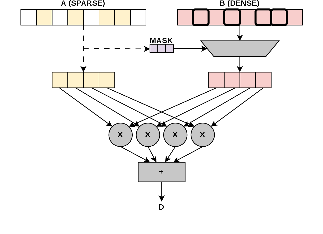
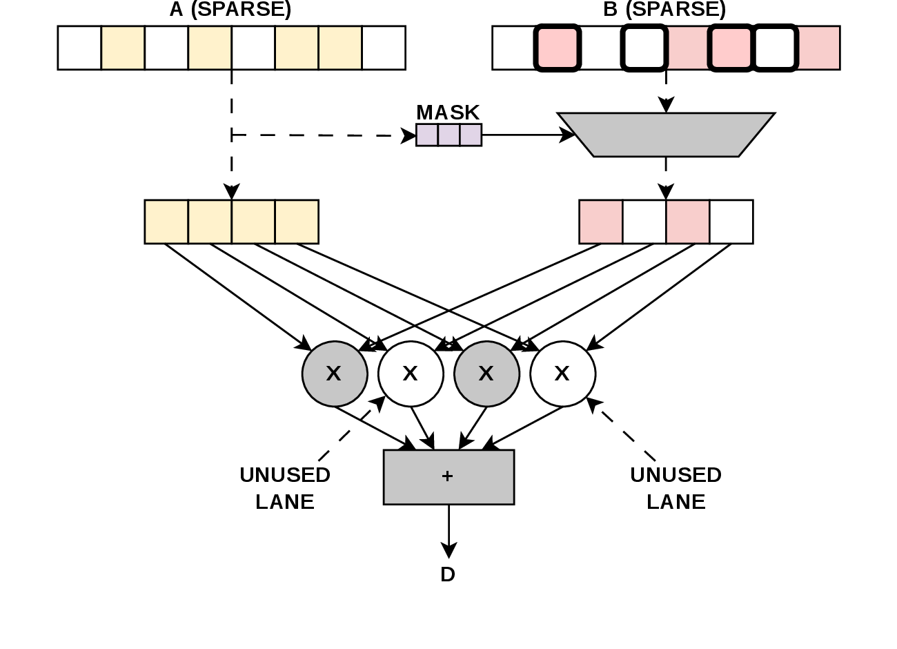
Figure 3: Inner-product primitive dual-side sparsity limitations.
Wang et al. proposed Dual-Side Sparse Tensor Cores (DSTC) [39] that circumvent this limitation by replacing the inner-dot-product units with outer-dot-product units. Outer-products naturally avoid the inner-join problem by computing cross-products between column-row vector pairs, thereby condensing sparse inputs into dense vectors before multiplication. However, outer-product requires storing full M\(\times\)N intermediate partial matrices in expensive accumulation buffers across K reduction steps, incurring substantial area overhead and reduced computational density for a given die.
Ten-Four adopts a pragmatic middle ground by retaining the area-efficient inner-product FEDP design while at least leveraging sparsity for power reduction through selective lane clock gating. As shown in Fig. 2, an input valid mask derived from the source operand format and zero-detection logic controls the clock gating of FEDP lanes. When a lane’s input is identified as zero, its pipeline registers are clock-gated from the very start, eliminating switching activity through the multiply and align stages where lane computations are self-contained. However, before entering the accumulator stage where multi-lane reduction occurs, the third pipeline registers’ outputs are AND-gated with the valid lane mask, ensuring disabled lanes provide zeros to the CSA rather than stale register values. This approach reduces dynamic power consumption without the microarchitectural complexity or area overhead of outer-product designs, making it a practical solution for Tensor Cores targeting dual-side sparse workloads. Notably, this scheme is orthogonal to 2:4 structured sparsity (whose speedup and power savings come from halving WMMA micro-ops in the \(K\)-dimension), and can be applied alongside it.
3.5 Microscaling (MX) Format Support↩︎
Block-floating-point formats preserve higher model accuracy than per-tensor quantization while retaining the memory and throughput benefits of low-precision arithmetic [12], [40]. The OCP MX specification [11] leaves the dot product’s internal precision and operation order as implementation-defined, allowing for aggressive microarchitectural flexibility.
The conventional approach adds the two E8M0 scale factors \(X^{(A)}\) and \(X^{(B)}\), removes FP32 bias (\(-254\)), and applies them to the sum-of-products (SoP) before final accumulation: \[D = X^{(A)} X^{(B)} \sum_{i=1}^{k} \left(A_i \times B_i \right) + C\] This deferred scaling is incompatible with Ten-Four’s pipeline, since the addend \(C\) is processed alongside the SoP from Stage 1. Ten-Four resolves this by simply rearranging the factorization of the scale factors as: \[D = \sum_{i=1}^{k} \left[ X^{(A)} X^{(B)} \left(A_i \times B_i \right) \right] + C\] This per-lane scale-factor compensation scheme, combined with the existing low-precision exponent and bias circuitry, enables MXFP8, MXBF8, and MXINT8 support with bare minimal modifications, as illustrated in Fig. 2.
4 Evaluation↩︎
4.1 FPGA Design Flow Analysis↩︎
We evaluate Ten-Four against equivalent Xilinx DSP IP, Berkeley HardFloat [17] and FPnew [19] based discrete TCU implementations, targeting 300 MHz operational clock frequency on the AMD Xilinx Alveo U55C FPGA [41] across a range of threads/warp configurations (NT = 4, 8, 16, 32).
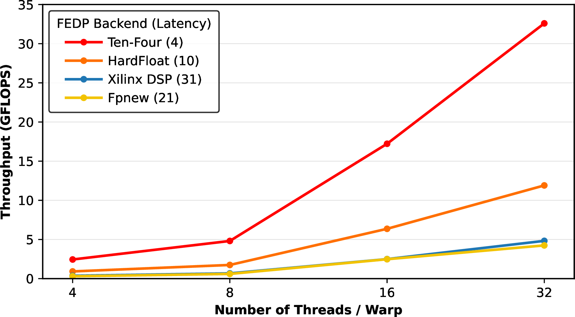
Fig. 4 shows that Ten-Four achieves significantly higher single-cycle throughput2 scaling (2.446–32.592 GFLOPS) compared to HardFloat (0.922–11.903 GFLOPS, \(\sim\)2.7\(\times\)), Xilinx DSP (0.367–4.824 GFLOPS, \(\sim\)6.7\(\times\)), and FPnew (0.304–4.244 GFLOPS, \(\sim\)7.9\(\times\)). This improvement largely stems from our 4-cycle latency and MOD-4 grouping CSA.
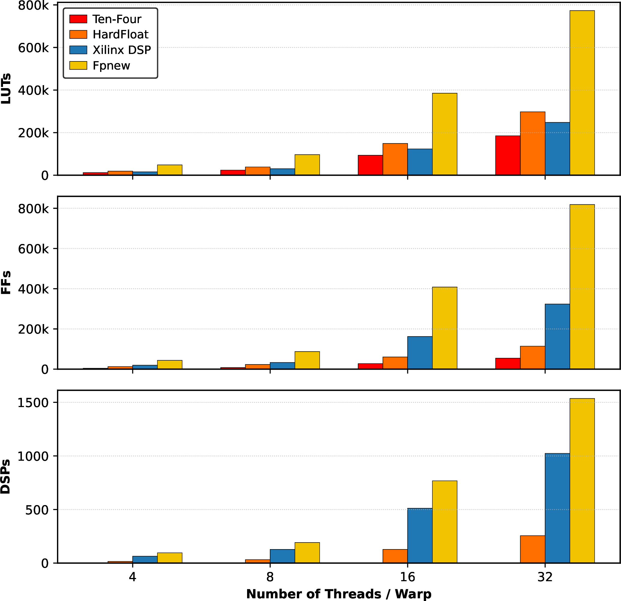
As demonstrated in Fig. 5, Ten-Four achieves 37–38% LUT reduction versus HardFloat, 24–25% versus Xilinx DSP, and 75–76% versus FPnew, despite eliminating DSP block usage entirely. Flip-Flop usage is also reduced by 52–66% compared to HardFloat, 75–83% compared to Xilinx DSP, and 90–93% compared to FPnew.
4.2 Dual-Side Sparse Lane Mask Power Analysis↩︎

We evaluate the sparse lane mask clock-gating scheme by sweeping dual-side sparsity from 0–100% in 10% steps across all supported formats on a 64x64x64 SGEMM kernel, using post-implementation SAIF-based power estimation on the Alveo U55C
FPGA. While Static power remains nearly constant (\(\sim\)3.30–3.39 W) across all formats and sparsity levels, as shown in Fig. 6, FP16 exhibits the highest dynamic power consumption (\(\sim\)5.2 W). TF32 and BF16 draw slightly less power due to their alternate-lanes-active-only scheme and smaller mantissa bit-width respectively. FP8/BF8 and integer formats consistently consume the least due to their leaner
multiplier logic. Notably, however, INT4 can exceed INT8 dynamic power beyond 70% sparsity levels, because its finer-granularity lane mask introduces proportionally higher clock-gating control overhead relative to the reduced compute activity.
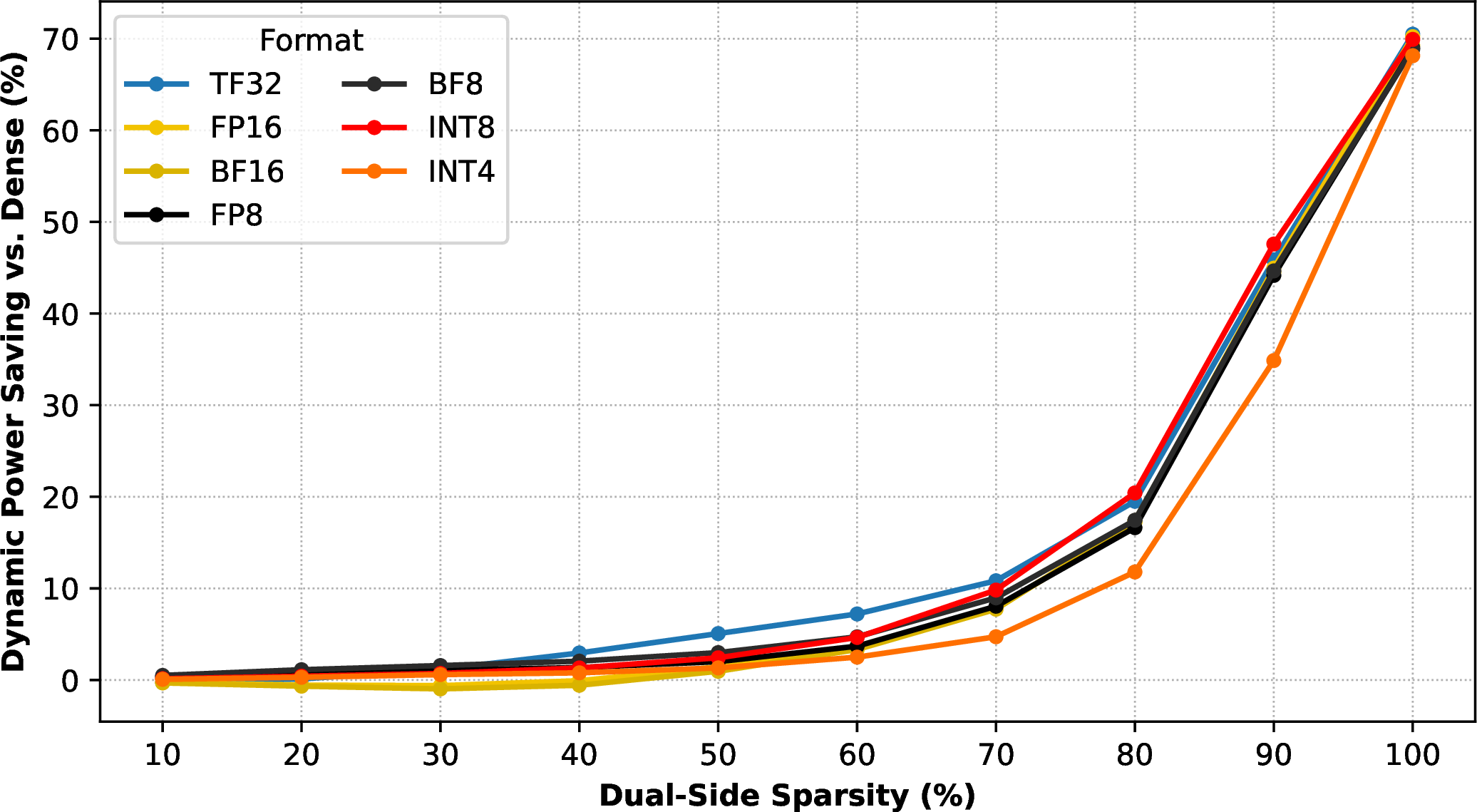
Fig. 7 demonstrates the corresponding dynamic power savings over the dense baseline. The sparse lane mask becomes increasingly compelling beyond 70% dual-side sparsity, improving from 4.7–10.8% savings at 70% to 34.9–47.6% at 90% and 68.1–70.5% at 100%. These results show that sparse lane clock-gating is an effective mechanism, that can be coupled with existing 2:4 structured sparsity schemes, to exploit dynamic power reduction in dual-side sparse workloads with bare minimal overhead.
4.3 ASIC Design Flow Analysis↩︎
To validate Ten-Four’s practical feasibility, we synthesize both four-element (NT=4,8) and eight-element (NT=16,32) dot product configurations using Synopsys Design Compiler and the ASAP7 7nm Predictive PDK [42]. Each configuration is synthesized in two variants: a minimal MXFP8/MXBF8-only datapath to establish a lean area baseline, and a fully-featured variant with all
floating-point and integer formats enabled to capture the overhead of format-wise shared logic fanout. All runs target the asap7sc7p5t_AO_LVT_TT_nldm standard cell library at 1500 MHz under PVT_0P7V_25C typical conditions.
Table 1 compares Ten-Four against prior FP8 dot-product accelerator designs.
| Design | Tech. | Voltage | Freq. | Area | Throughput | Scale |
| nm | V | GHz | mm\(^2\) | GFLOPS | Support | |
| ExSdotp [27] | 12 | 0.8 | 1.26 | \(5.13 \times 10^{-3}\) | 20.2 | |
| Desrentes et al. [29] | 16 | — | 1.25 | \(9.81 \times 10^{-3}\) | 80.0 | |
| Lutz et al. [31] | 5 | — | 3.6 | \(6.74 \times 10^{-4}\) | 28.8 | \((1 \times 7\mathrm{b})\) |
| MXDOTP [32] | 12 | 0.8 | 1.09 | \(3.15 \times 10^{-3}\) | 17.4 | \((2 \times 8\mathrm{b})\) |
| Ten-Four (Ours) | 7 | 0.7 | 1.66 | \(\mathbf{1.06 \times 10^{-3}}\) | 26.6\(\dagger\) | \(\mathbf{(2 \times 8\mathrm{b})}\) |
| 1.55 | \(\mathbf{1.93 \times 10^{-3}}\) | 49.6\(\ddagger\) | ||||
| Ten-Four (All fmts) | 7 | 0.7 | 1.58 | \(\mathbf{2.40 \times 10^{-3}}\) | 25.2\(\dagger\)* | \(\mathbf{(2 \times 8\mathrm{b})}\) |
| 1.58 | \(\mathbf{4.65 \times 10^{-3}}\) | 50.4\(\ddagger\)* |
1.5pt

A single Ten-Four-based Tensor Core delivers up to 404.5 GFLOPS of TF32, 808.9 GFLOPS of FP16/BF16, and 1.617 TFLOPS of FP8/BF8 at 291.92 mW, yielding a peak efficiency of \(\sim\)2.771 TFLOPS/W at NT=32. Under a technology-normalized, iso-configuration comparison against NVIDIA’s A100 Architecture [9] (also known to be 7nm, \(\sim\)720 GFLOPS of FP16/BF16 per Tensor Core at 1410 MHz boost clock from publicly available documents), Ten-Four achieves \(\sim\)12.3% higher per-unit peak throughput while supporting a significantly broader format and feature range. The power-density grid and GDS layout successfully exported from Synopsys ICC2 place-and-route are shown in Fig. 8.
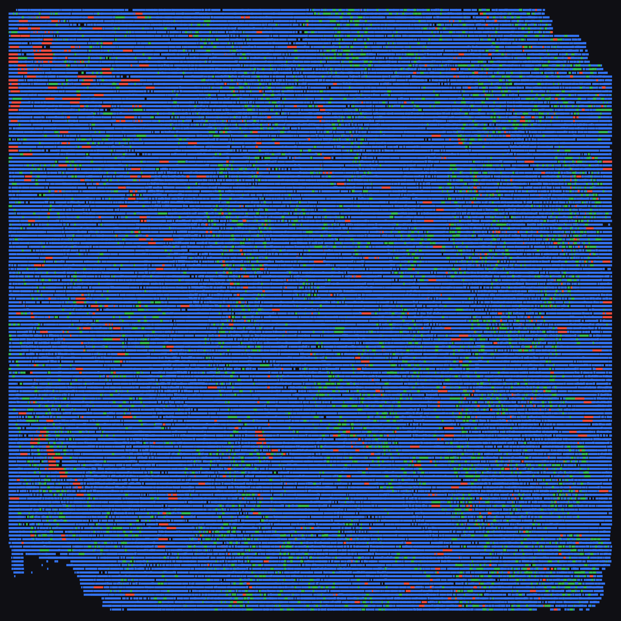
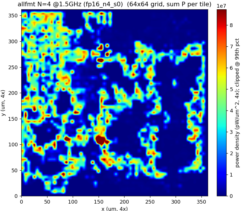
Figure 8: Ten-Four FEDP ASIC physical design analysis.
4.4 Numerical Accuracy Verification↩︎
To validate Ten-Four’s FEDP computation, we develop a verification framework using PyTorch-based CUDA kernel generation to produce format-specific WMMA and PTX routines targeting NVIDIA’s Ada Architecture [38] RTX 4090 GPUs as the hardware reference. Our verification harness systematically exercises corner cases across six distinct feature classes: normals, subnormals, zeros, infinities, NaNs and catastrophic cancellation scenarios. Ten-Four produces bit-exact results matching the NVIDIA Ada Tensor Core outputs for all supported floating-point (TF32, FP16, BF16, FP8, and BF8), and integer (INT8 and INT4) formats, across all 1,000,000+ randomized test vectors.
We further port the FTTN benchmark [43] through the Vortex WMMA C++ API to verify IEEE-compliant subnormal handling and rounding, and compare Ten-Four’s precision characteristics against analytical numerical accuracy models of commercial GPUs [44], as summarized in Table ¿tbl:tab:fp-behavior?.
3.9pt
llccccc Inputs & GPU & & & Acc. & &
& H100 & & \((2,13)\) & 21 & 32 & Trunc.
& B200 & & \((2,25)\) & 33 & 32 & Trunc.
& Ten-Four & & \(\mathbf{(2,25)}\) & 30 & 16 & RTN-TE
& V100 & & \((2,23)\) & 28 & 4 & Trunc.
& A100 & & \((2,24)\) & 30 & 8 & Trunc.
& H100 & & \((2,25)\) & 32 & 16 & Trunc.
& B200 & & \((2,25)\) & 32 & 16 & Trunc.
& Ten-Four & & \(\mathbf{(2,25)}\) & 30 & 8 & RTN-TE
& A100 & & \((2,24)\) & 29 & 4 & Trunc.
& H100 & & \((2,25)\) & 31 & 8 & Trunc.
& B200 & & \((2,25)\) & 31 & 8 & Trunc.
& Ten-Four & & \(\mathbf{(2,25)}\) & 30 & 4 & RTN-TE
4.5 TCU Extended SGEMM Kernel Roofline Analysis↩︎
Finally, we perform roofline modeling on a 256x256x256 SGEMM kernel across all Ten-Four supported formats, using a Vortex configuration equivalent to a single NVIDIA SM (1 socket, 4 cores, 16 warps, 32 threads). As illustrated in Fig. 9, the FP32 baseline relying on the FPU remains memory-bound, reaching only 2.3% compute utilization even at this relatively small kernel size. In contrast, Ten-Four enabled TCUs move the kernel beyond the ridge point and
into the compute-bound region for all low-precision formats. Compute utilization progressively increases from 16.0% for TF32 to 29.1% for FP16/BF16, 51.1% for FP8/BF8, and 47.8% for MXFP8/MXBF8. While the corresponding operational intensities also improve,
they remain well below the ideal \(N/6=42.7\) FLOP/byte value.

Notably, the achieved throughput does not scale perfectly by 2\(\times\) when moving from TF32 to FP16/BF16 or from FP16/BF16 to FP8/BF8, since the kernel still incurs non-arithmetic overheads from warp scheduling, instruction issue, and register and memory traffic. MXFP8/MXBF8 slightly trails plain FP8/BF8 due to scale-factor metadata accesses, which introduce overhead beyond the arithmetic datapath.
5 Conclusion↩︎
In this paper, we introduced Ten-Four, an open-source high-performance Fused Dot Product Unit microarchitecture for developing a feature-rich mixed-precision Tensor Core Unit Extension to the RISC-V based Vortex GPGPU. By fusing the Integer and Floating-Point datapath, clock-gating sparse lanes and performing Microscaling with early addend accumulation, Ten-Four overcomes the latency and resource utilization limitations of current discrete arithmetic unit based FEDP designs for Tensor Cores. We achieved 4-cycle operation latency at 300 MHz, delivering 130.368 GFLOPS peak throughput per Tensor Core on the Xilinx U55C FPGA, while also matching NVIDIA Tensor Core numerical accuracy. ASIC synthesis in 7nm FinFET achieves 1.58 GHz \(F_{\text{max}}\) and 2.771 TFLOPS/W peak efficiency, exceeding NVIDIA A100’s per-unit throughput by \(\sim\)12.3% at an iso-configuration. Ten-Four’s low-precision format support also enables pushing SGEMM kernels from memory-bound to compute-bound regions. Furthermore, Ten-Four’s configurable RTL design and verification methodology enables rapid prototyping and evaluation of custom block-quantized and unstructured sparse formats for hardware-software co-design of deep learning inference accelerators in the future.